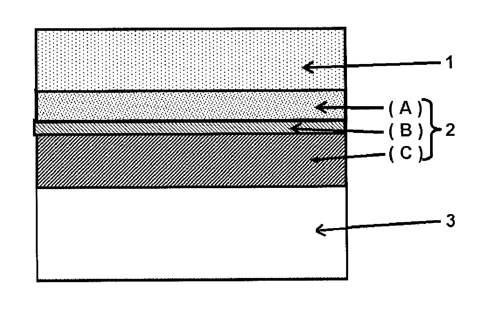
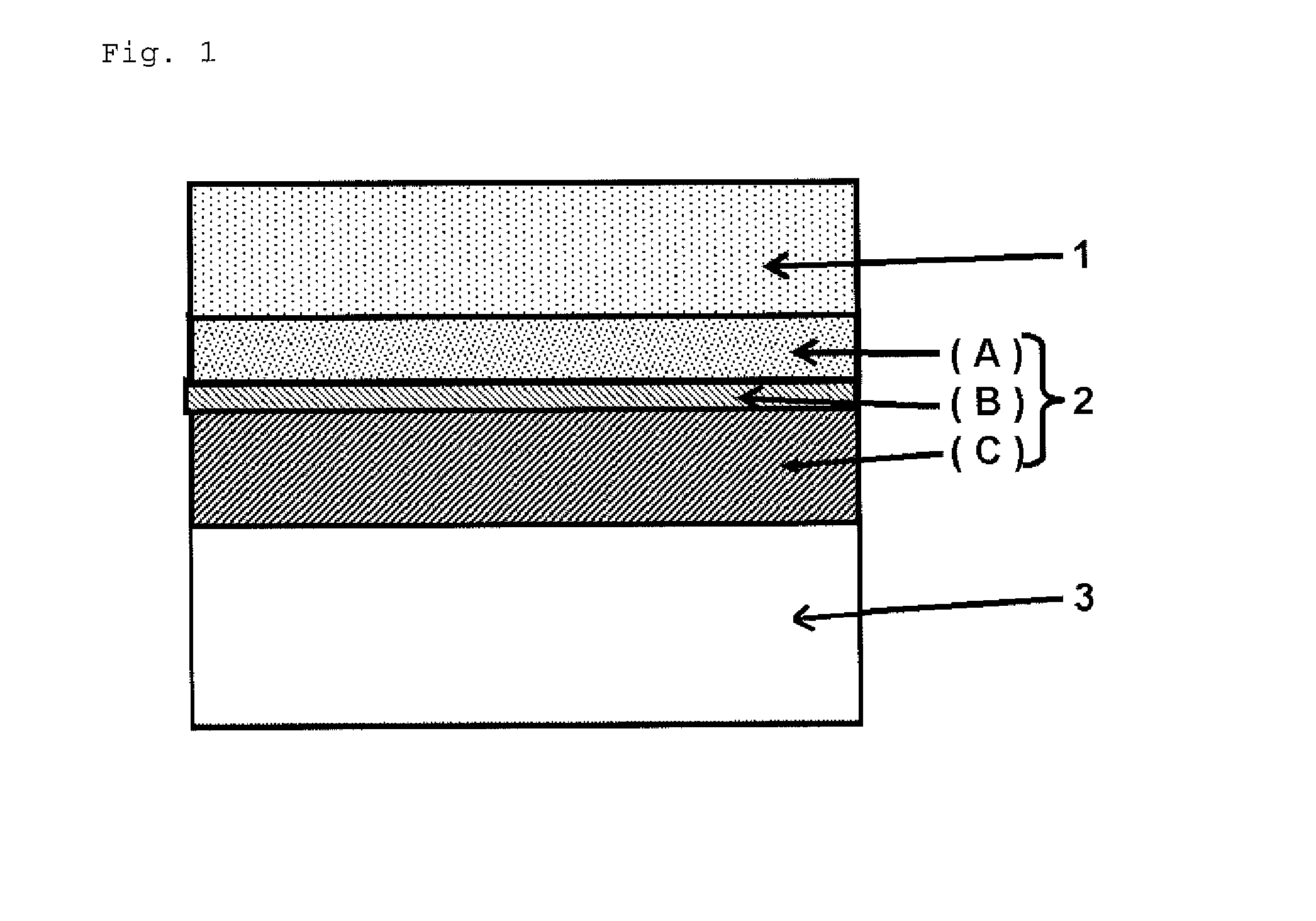
Wafer processing laminate, wafer processing member, temporary adhering material for processing wafer, and manufacturing method of thin wafer
a technology of wafers and adhesives, applied in the direction of film/foil adhesives without carriers, transportation and packaging, layered products, etc., can solve the problems of insufficient strength and heat resistance, long treatment time per one substrate, and expensive laser tools, etc., to achieve high heat resistance, easy manufacturing, and high uniform thickness
- Summary
- Abstract
- Description
- Claims
- Application Information
AI Technical Summary
Benefits of technology
Problems solved by technology
Method used
Image

Examples
example 1
Resin Synthetic Example 1
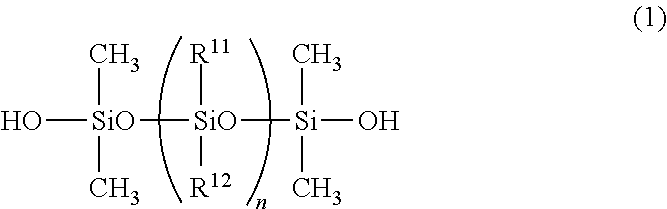
[0104]In a four-necked flask, 90 parts of dimethylpolysiloxane which is a crude rubber state dimethylpolysiloxane (in the formula (1), “n” represents 9000) both of the molecular ends of which have been sealed by hydroxyl groups, and a viscosity of a 30% toluene solution thereof at 25° C. is 98,000 mPa·s, and 10 parts of a methylpolysiloxane resin comprising 0.75 mol of a (CH3)3SiO1 / 2 unit and 1 mol of an SiO4 / 2 unit, and containing 1.0 mol % of a hydroxyl group in 100 of a solid component were dissolved in 900 parts of toluene. To the obtained solution was added 1 part of 28% aqueous ammonia, and the mixture was subjected to condensation reaction under stirring at room temperature for 24 hours. Then, the resulting mixture was heated to 180° C. under the state of a reduced pressure, and toluene, condensed water, ammonia, etc., were removed therefrom to obtain a solidified partially condensed product. 900 parts of toluene was added to 100 parts of the partiall...
example 2
Resin Synthetic Example 2
[0106]In a four-necked flask, 95 parts of dimethylpolysiloxane which is a crude rubber state dimethylpolysiloxane (in the formula (1), “n” represents 9000) both of the molecular ends of which have been sealed by hydroxyl groups, and a viscosity of a 30% toluene solution thereof at 25° C. is 98,000 mPa·s, and 5 parts of a methylpolysiloxane resin comprising 0.75 mol of a (CH3)3SiO1 / 2 unit and 1 mol of an SiO4 / 2 unit, and containing 1.0 mol % of a hydroxyl group in 100 of a solid component were dissolved in 900 parts of toluene. To the obtained solution was added 1 part of 28% aqueous ammonia, and the mixture was subjected to condensation reaction under stirring at room temperature for 24 hours. Then, the resulting mixture was heated to 180° C. under the state of a reduced pressure, and toluene, condensed water, ammonia, etc., were removed therefrom to obtain a solidified partially condensed product. 900 parts of toluene was added to 100 parts of the partially...
example 3
Resin Synthetic Example 3
[0108]In a four-necked flask were charged 1,000 g (3.38 mol) of octamethylcyclotetrasiloxane and 0.24 g (0.0015 mol) of hexamethyldisiloxane, and a temperature of the mixture was maintained at 110° C. Then, 4 g of 10% by mass tetrabutylphosphonium hydroxide siliconate was added to the mixture and the mixture was polymerized over 4 hours, and a post-treatment was carried out at 160° C. for 2 hours to obtain dimethylpolysiloxane.
[0109]When the ratio of the D unit and the M unit of the dimethylpolysiloxane was examined by the 29Si-NMR method, the D unit was 99.978% and the M unit was 0.022%, whereby it could be identified as the dimethylpolysiloxane having the following structure and the polymerization degree of about 9,000.
[0110]500 g of the dimethylpolysiloxane was dissolved in 500 g of hexane, and the solution was added to 2 L of acetone, and the precipitated resin was recovered. Thereafter, hexane, etc., were removed under vacuum to obtain a dimethylpolysil...
PUM
| Property | Measurement | Unit |
|---|---|---|
| thickness | aaaaa | aaaaa |
| thickness | aaaaa | aaaaa |
| molar ratio | aaaaa | aaaaa |
Abstract
Description
Claims
Application Information
 - R&D
- Intellectual Property
- Life Sciences
- Materials
- Tech Scout
- Unparalleled Data Quality
- Higher Quality Content
- 60% Fewer Hallucinations
Browse by: Latest US Patents, China's latest patents, Technical Efficacy Thesaurus, Application Domain, Technology Topic, Popular Technical Reports.
© 2025 PatSnap. All rights reserved.Legal|Privacy policy|Modern Slavery Act Transparency Statement|Sitemap|About US| Contact US: help@patsnap.com