

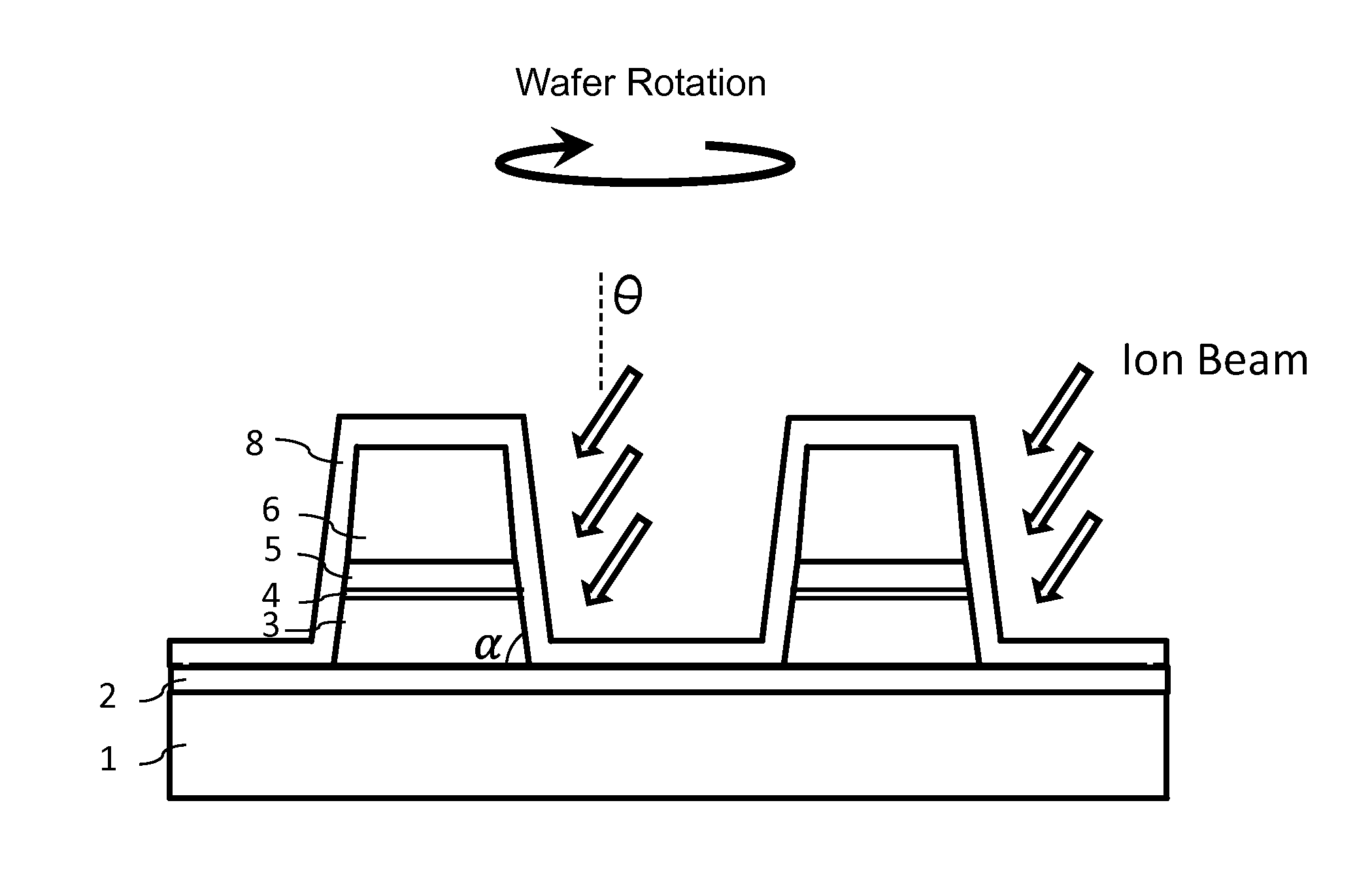
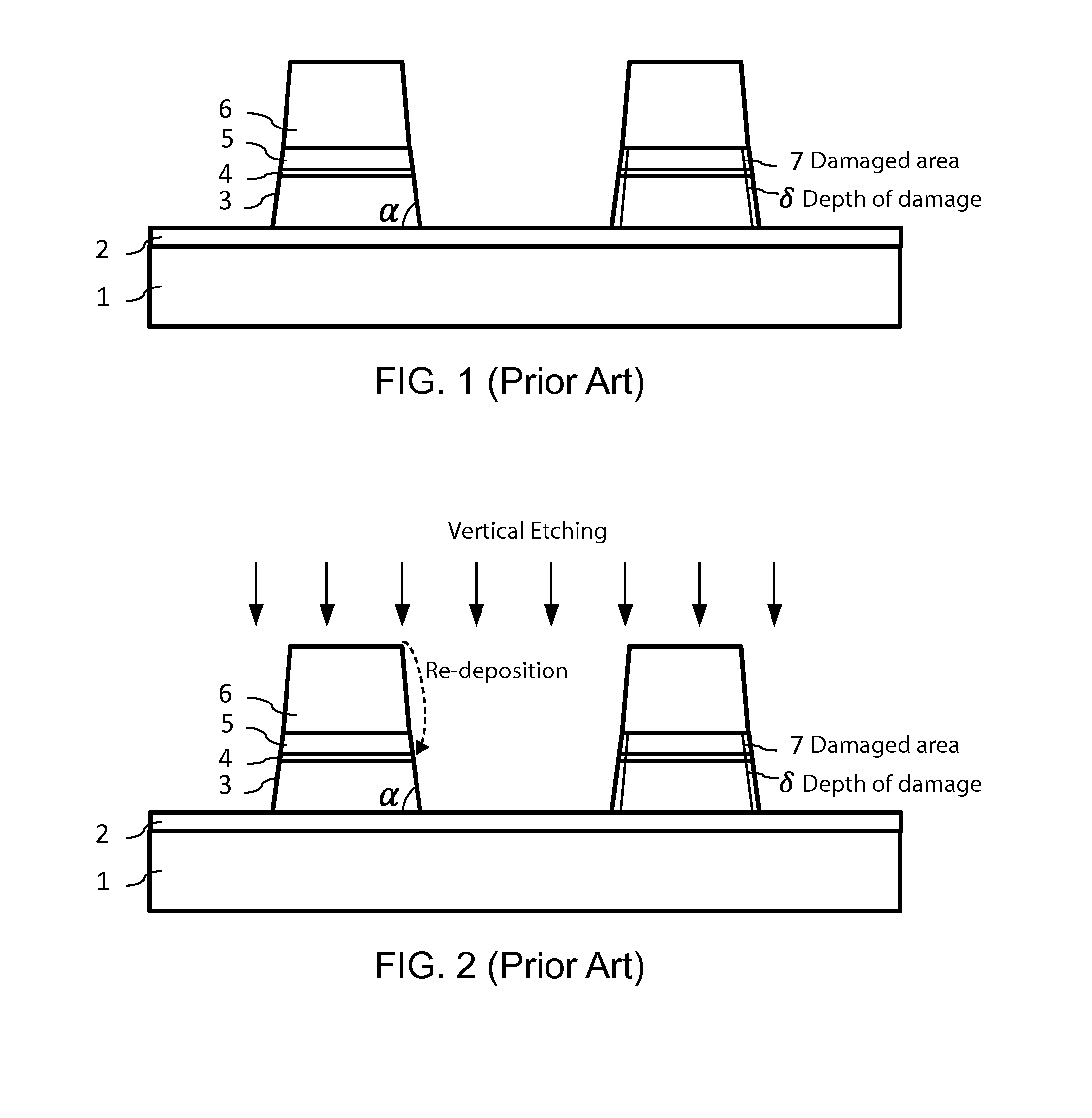
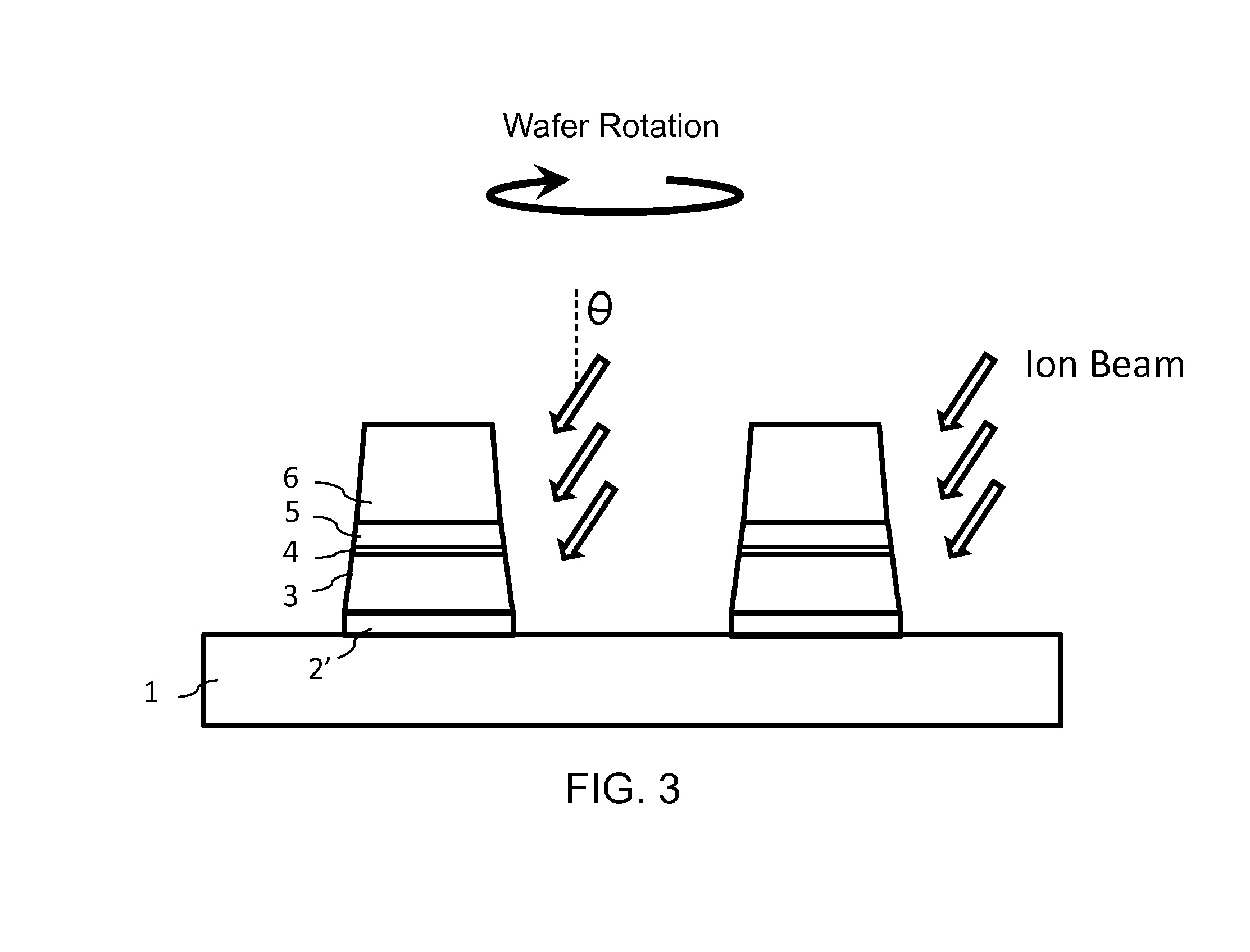
Mtj stack and bottom electrode patterning process with ion beam etching using a single mask
a technology of etching process and mask, which is applied in the manufacture/treatment of galvano-magnetic devices, basic electric elements, electric devices, etc., can solve the problems of re-deposition of etched material on the sidewall, difficult to find a hard mask material with enough selectivity for use with rie, and inability to control the size of mtj and its uniformity for scalability. , to achieve the effect of improving selectivity
- Summary
- Abstract
- Description
- Claims
- Application Information
AI Technical Summary
Benefits of technology
Problems solved by technology
Method used
Image

Examples
first embodiment
[0037]An alternative of the first embodiment separates the IBE bottom electrode etching into 2 steps as shown in FIGS. 4A & 4B. In FIG. 4A the 1st step is designed to remove the exposed bottom electrode material with a first angle which is preferably a low angle of incidence (e.g. close to normal) selected to efficiently remove the unneeded bottom electrode material. In some cases, a higher etching angle is effective to remove the bottom electrode but is susceptible to re-deposition. As shown in FIG. 4B, the 2nd step is to clean the sidewall with a second incident angle, higher than the first angle.
[0038]Variations of the first embodiment include etching the MTJ stack with processes with reduced chemical damage including ICP using inert gas such as Ar or Kr, or a mixture of Ar or Kr with other gases such as CH3OH, CO, NH3, etc. This step is followed by the bottom electrode etching with angle IBE for sidewall re-deposition cleaning.
[0039]Etch rate of RIE including MICP using inert ga...
second embodiment
[0040]the invention illustrated in FIG. 5 adds to the first embodiment and its alternatives by including MTJ sidewall protection by depositing passivation layer 8 over the etched MTJ layer stacks and the unetched bottom electrode layer 2 prior to commencing the bottom electrode etching process. The passivation layer 8 can be a material such as a nitride. The passivation layer 8 protects the barrier layer from re-deposition during the bottom electrode IBE with incident angles normal or close to normal. The passivation layer 8 in this embodiment avoids the barrier layer exposed to air when vacuum is broken in some embodiments. The passivation layer 8 is consumed during the IBE process.
[0041]FIG. 6 illustrates an alternative embodiment in which the MTJ etching is separated into two stages. The first stage proceeds with RIE etching until the barrier layer 4′ is exposed as shown in FIG. 6. At this point angled IBE etching is commenced as shown in FIG. 6. Remaining MTJ layers in the stack...
third embodiment
[0042]the invention includes self-adjustment of MTJ CD (Critical Dimension) with angled IBE. Etch rate of IBE depends on the specific materials as well as the incident angle as shown in FIG. 7. In this example the etch rate is highest at an incident angle of 50 degrees. The etch rate can be separated into vertical and horizontal components which vary with the incident angle of IBE. By varying the incident angle (a1, a2, a3), the bottom slope of MTJ can be changed as shown in FIG. 8 due to different etch rates. The higher angles, such a3, result in greater etching of the lower magnetic layer 3. The lowest angles, such a1 in this example, result in relatively less etching of the lower magnetic layer 3. By selecting an optimal angle, the slope of the bottom of the MTJ can be formed as steep as desired. Control of the slope of the bottom of the MTJ is advantageous for control the CD. A steep side wall makes it easier to control the CD.
[0043]FIG. 8 illustrates that the choice of IBE angl...
PUM
 Abstract
Description
Claims
Application Information