Thermally enhanced semiconductor assembly with embedded chip and interposer and method of manufacturing the same

Inactive Publication Date: 2014-06-26
BRIDGE SEMICON
View PDF0 Cites 12 Cited by
  • Summary
  • Abstract
  • Description
  • Claims
  • Application Information

AI Technical Summary

Benefits of technology

The present invention provides a method for attaching a chip and interposer to a heat sink using an adhesive. The method involves dispensing adhesive on the heat sink, inserting the chip into the cavity, and aligning an alignment guide with the chip and interposer. This alignment guide prevents lateral movement of the interposer or chip. The adhesive surrounds the chip and interposer, providing strong mechanical and thermal connections. The method improves manufacturing yield and provides reliable and cost-effective assembly for high volume manufacture.

Problems solved by technology

The convergence of mobility, communication, and computing has created significant thermal, electrical and cost challenges to the semiconductor packaging industry.
For instance, semiconductor devices are susceptible to performance degradation as well as short life span, and may encounter immediate failure at high operating temperatures.
In addition, semiconductor devices are often susceptible to undesirable electromagnetic interference (EMI) or other inter-device interference when they are densely packed together.
The signal integrity of these devices can be adversely affected when they perform high frequency transmitting or receiving.
As the heat sink is attached to the wiring board by adhesive or other mechanical means, any separation between the heat sink and the board would degrade the thermal performance of the chip.
Furthermore, as the heat sink is mechanically supported by the wiring board, the wiring board's thermal stability and rigidity often affect package's reliability.
Since the molding compound is typically a poor thermal conductor, the heat generated from the enclosed chip would be completely blocked.
Even though a portion of the molding compound can be removed to re-expose the chip and contacts external heat sink, the slow grinding process of removing the hardened molding compound can be expensive.
Also, the assembly may suffer moisture penetration, voids and cracks at the chip interfaces which may cause serious reliability concerns.
However, even though thermal issue can be resolved, applying a pressure of about 370 kg / cm2 at a temperature of 100° C. to 200° C. to press the chip into the metal block is prohibitively cumbersome and prone to damage the chip.
Furthermore, since there is no bonding material to accurately position and secure the embedded chip, voids and inconsistent bond lines arise between the chip and the heat slug.
As a result, the assembly suffers from high yield loss, poor reliability and excessive cost.
However, since the build-up circuitry is directly formed on the chip surface and connected to the chip contact pad through microvia or post, the depth control of the metal cavity which dictates the co-planarity of the chip with the metal surface becomes extremely critical.
Any protrusion or recess of the chip from the metal surface will affect the via / post reliability and may cause electrical disconnection between the chip and the build-up layers.
Furthermore, as the semiconductor chip is placed in the cavity by adhesive or solder, lateral movement of the chip during die attach process often results in via / pad misalignment.

Method used


Image

  • Thermally enhanced semiconductor assembly with embedded chip and interposer and method of manufacturing the same
  • Thermally enhanced semiconductor assembly with embedded chip and interposer and method of manufacturing the same
  • Thermally enhanced semiconductor assembly with embedded chip and interposer and method of manufacturing the same

Examples


embodiment 1

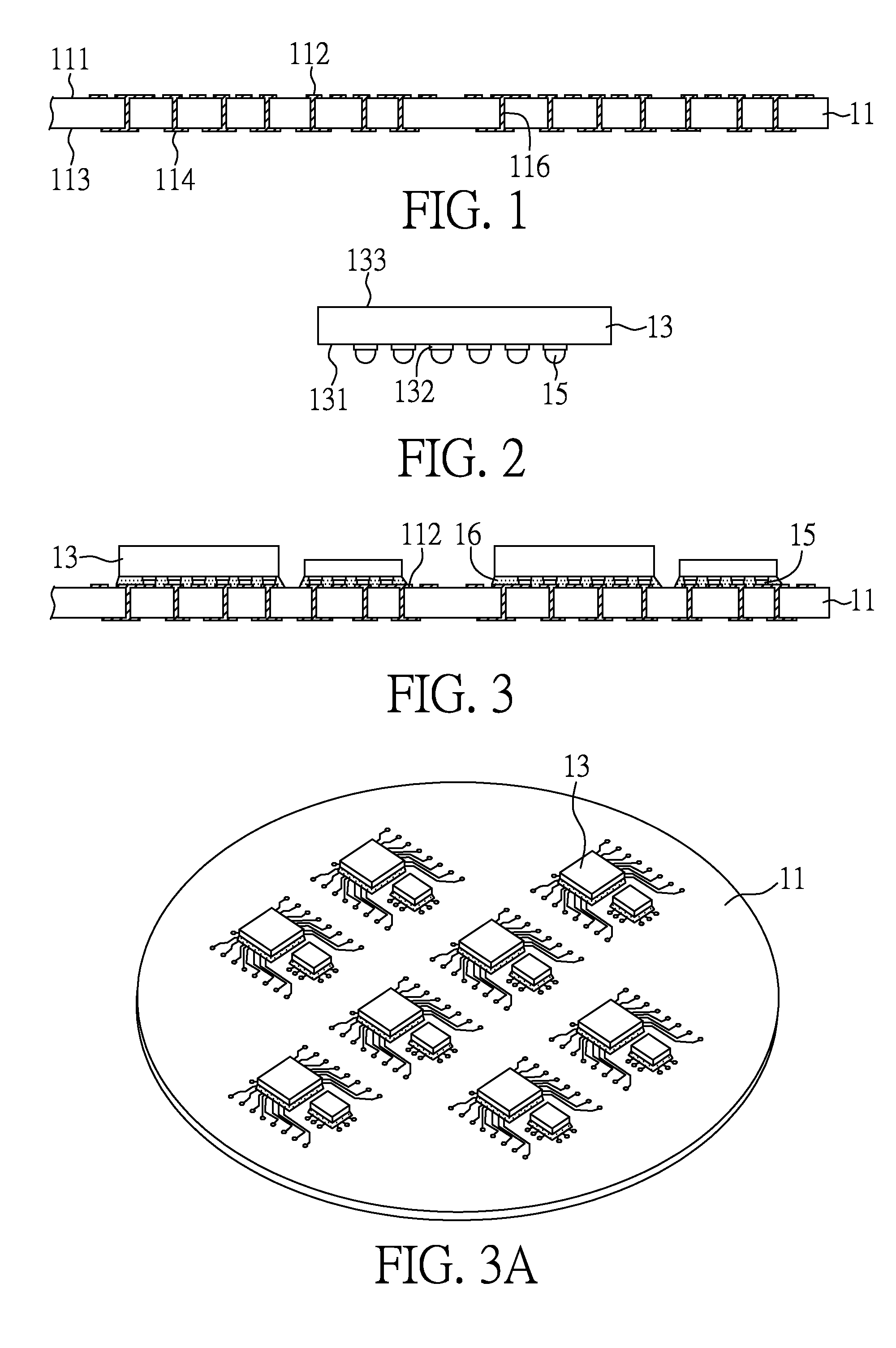
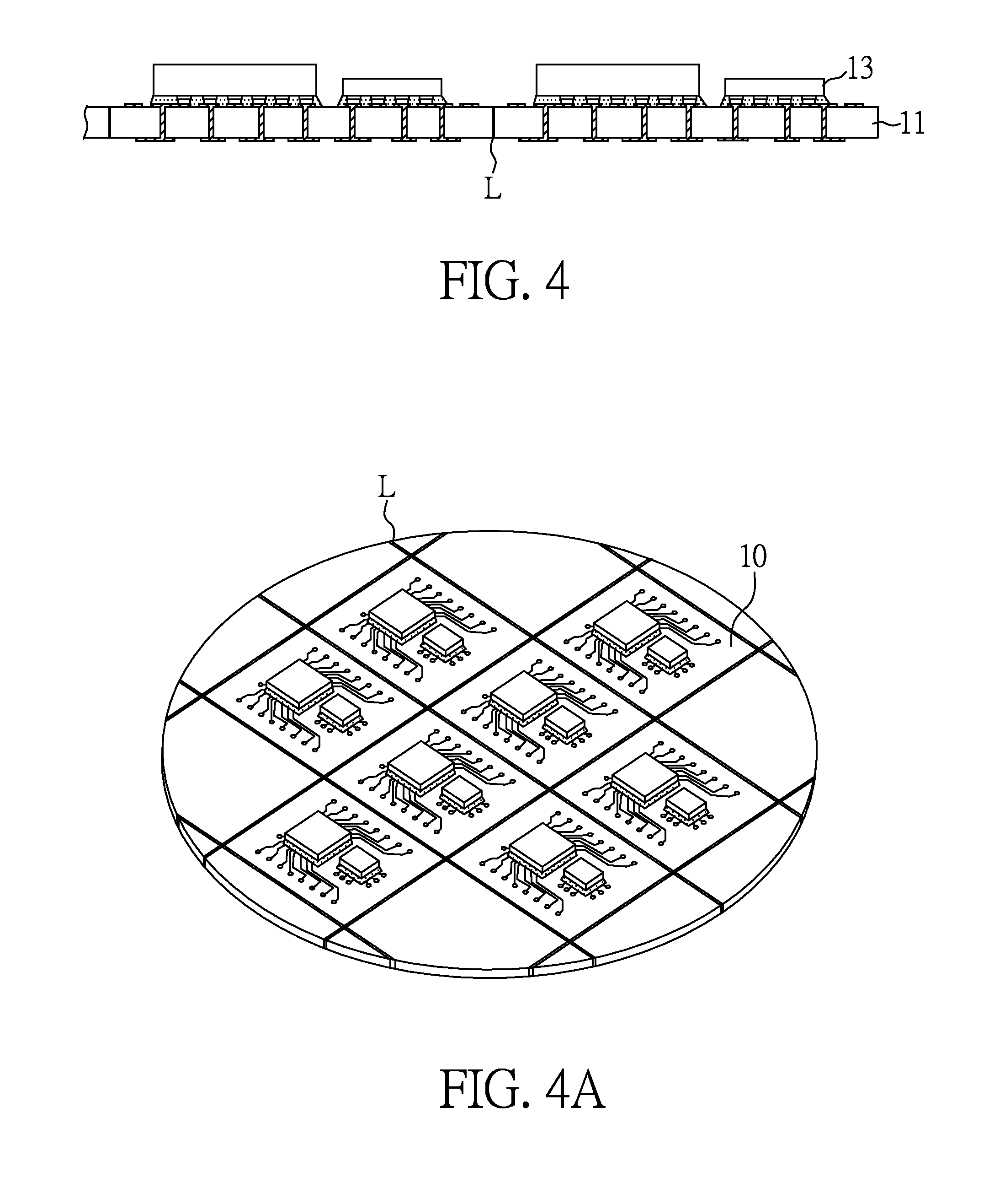
[0045]FIGS. 1-14 are cross-sectional views showing a method of making a thermally enhanced semiconductor assembly that includes an interposer, chips, a heat sink and build-up circuitry in accordance with an embodiment of the present invention.

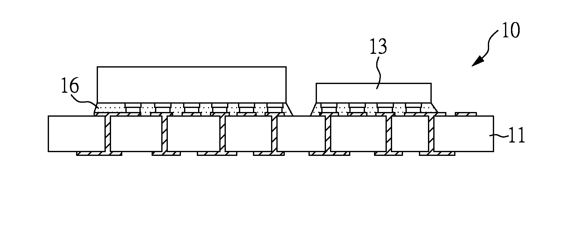
[0046]As shown in FIG. 14, semiconductor assembly 110 includes interposer 11, chips 13, heat sink 20 and build-up circuitry 30. Interposer 11 and chips 13 are attached on heat sink 20 using adhesive 19 with chips 13 embedded in cavities 211 of heat sink 20 and alignment guide 213 laterally aligned with peripheral edges of interposer 11. Alignment guide 213 extends beyond first surface 111 of interposer 11 in the upward direction and is in close proximity to peripheral edges of interposer 11. Build-up circuitry 30 covers interposer 11 and heat sink 20 in the upward direction and is electrically coupled to second contact pads 114 of interposer 11 through first conductive vias 317.

[0047]FIGS. 1-5 are cross-sectional views showing a process of fabr...

embodiment 2

[0068]FIGS. 15-19 are cross-sectional views showing a method of making another thermally enhanced semiconductor assembly with additional conductive vias in contact with the heat sink in accordance with another embodiment of the present invention.

[0069]For purposes of brevity, any description in above Embodiment is incorporated herein insofar as the same is applicable, and the same description need not be repeated.

[0070]FIGS. 15 and 15A are cross-sectional and top perspective views, respectively, of heat sink 20 with alignment guide 213 around entrance of cavity 211. Alignment guide 213 can be formed by removing selected portions of metallic base sheet 21 or by pattern deposition including electroplating, electroless plating, evaporating, sputtering and their combinations using photolithographic process. In this illustration, as shown in FIG. 15A, alignment guide 213 laterally extends to the peripheral edges of heat sink 20 and has inner peripheral edges that conforms to four sides o...

embodiment 3

[0076]FIGS. 20-26 are cross-sectional views showing a method of making yet another thermally enhanced semiconductor assembly with an laminate substrate as the heat sink in accordance with yet another embodiment of the present invention.

[0077]For purposes of brevity, any description in above Embodiments is incorporated herein insofar as the same is applicable, and the same description need not be repeated.

[0078]FIGS. 20 and 21 are cross-sectional views showing a process of forming an alignment guide on a dielectric layer of a laminated substrate in accordance with an embodiment of the present invention, and FIG. 21A is a top perspective view corresponding to FIG. 21.

[0079]FIG. 20 is a cross-sectional view of a laminate substrate that includes metallic base sheet 21, dielectric layer 23 and metal layer 25. Dielectric layer 23 is sandwiched between metallic base sheet 21 and metal layer 25. Dielectric layer 23 typically is made of epoxy resin, glass-epoxy, polyimide and the like and ha...


PUM


Abstract

The present invention relates to a method of making a thermally conductive semiconductor assembly. In accordance with a preferred embodiment, the method includes: providing a chip; providing an interposer that includes a through via, a first contact pad on a first surface and a second contact pad on an opposite second surface; electrically coupling the chip to the first contact pad of the interposer by a conductive bump or a wire; providing a heat sink with a cavity; then attaching the chip and the interposer on the heat sink using an adhesive with the chip inserted into the cavity; and then forming a build-up circuitry on the second surface of the interposer. Accordingly, the heat sink can provide essential thermal dissipation for the embedded chip, and the interposer and build-up circuitry can respectively provide first and second level fan-out routing / interconnection for the embedded chip.

Description

CROSS REFERENCE TO RELATED APPLICATION[0001]This application is a continuation-in-part of U.S. application Ser. No. 13 / 615,819 filed Sep. 14, 2012 and a continuation-in-part of U.S. application Ser. No. 13 / 753,625 filed Jan. 30, 2013, each of which is incorporated by reference. This application also claims the benefit of filing date of U.S. Provisional Application Ser. No. 61 / 895,506 filed Oct. 25, 2013.[0002]U.S. application Ser. No. 13 / 753,625 filed Jan. 30, 2013 is a continuation-in-part of U.S. application Ser. No. 13 / 615,819 filed Sep. 14, 2012. U.S. application Ser. No. 13 / 615,819 filed Sep. 14, 2012 and U.S. application Ser. No. 13 / 753,625 filed Jan. 30, 2013 all claim the benefit of filing date of U.S. Provisional Application Ser. No. 61 / 682,801 filed Aug. 14, 2012.BACKGROUND OF THE INVENTION[0003]1. Field of the Invention[0004]The present invention relates to a thermally enhanced semiconductor assembly and a method of making the same, more particularly, to a thermally enhan...

Claims


Application Information

Patent Timeline
IPC IPC(8): H01L23/367H01L23/00
CPCH01L24/97H01L23/3672H01L21/50H01L23/13H01L23/147H01L23/36H01L23/49827H01L23/49833H01L23/5389H01L24/13H01L24/16H01L24/32H01L24/48H01L24/73H01L24/81H01L24/83H01L24/92H01L2224/0401H01L2224/04105H01L2224/13144H01L2224/13147H01L2224/16225H01L2224/16227H01L2224/32225H01L2224/32245H01L2224/48091H01L2224/48227H01L2224/73204H01L2224/73253H01L2224/73265H01L2224/81203H01L2224/81207H01L2224/81815H01L2224/8314H01L2224/92125H01L2224/97H01L2924/00014H01L2924/12042H01L2924/181H01L2924/3025H01L2924/00012H01L2224/83H01L2224/81H01L2224/85H01L2924/00H01L2224/45099H01L2224/45015H01L2924/207
Inventor LIN, CHARLES W.C.WANG, CHIA-CHUNG
Owner BRIDGE SEMICON
Why Eureka
Try Eureka