

Photoresist pattern trimming methods
a technology of photoresist and pattern, applied in the field of electronic device manufacturing, can solve the problems of affecting the quality of photoresist, the inability to manufacture devices requiring greater resolution, and the difference in solubility characteristics between exposed and unexposed regions of resist,
- Summary
- Abstract
- Description
- Claims
- Application Information
AI Technical Summary
Benefits of technology
Problems solved by technology
Method used
Image

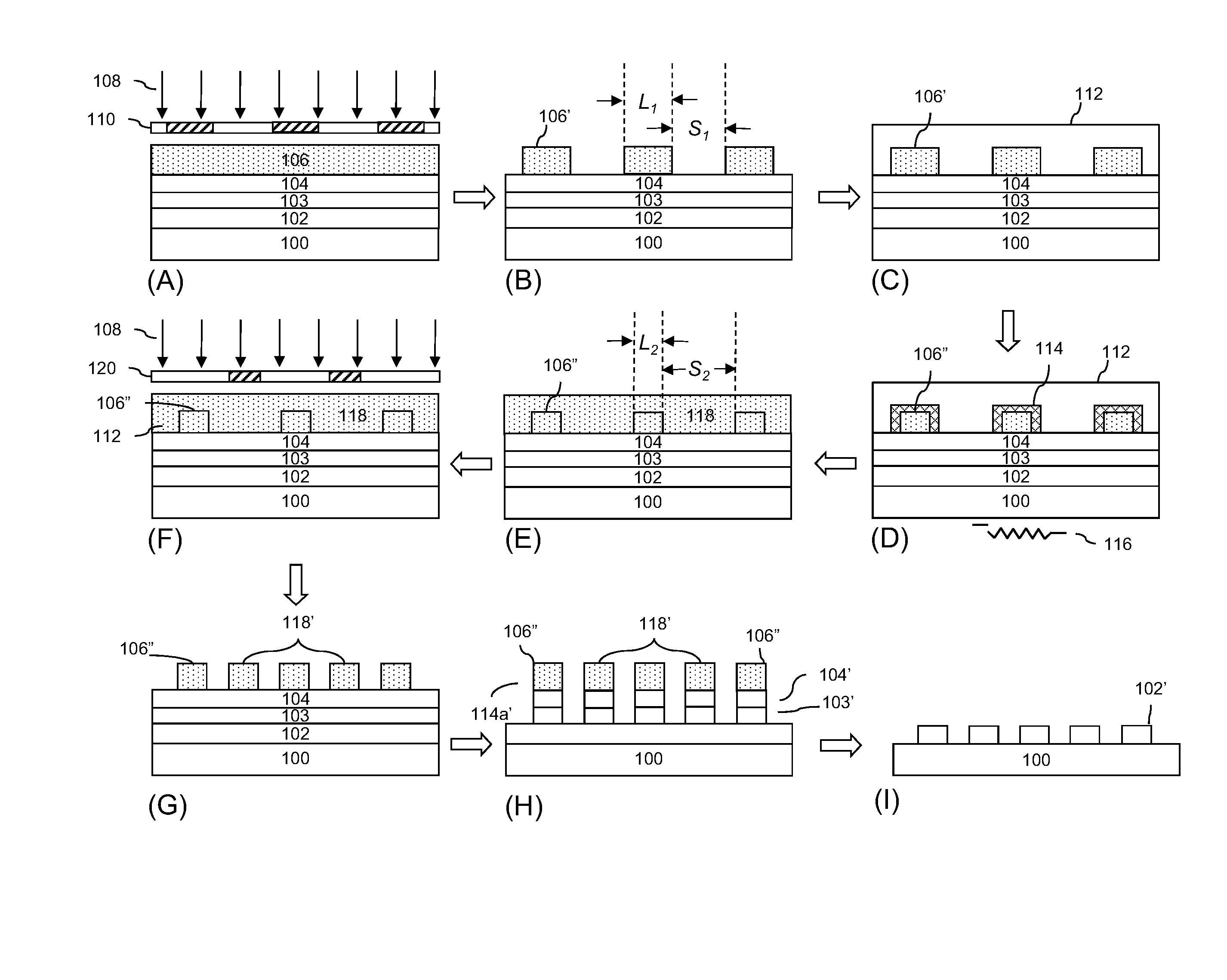
Examples
example 1
[0046]The following monomers M1-M4 were used to form polymers for the photoresist composition described below:
A positive chemically amplified photoresist composition was prepared by combining 1.28 g Polymer A (M1 / M2 / M3=4 / 4 / 2 mole ratio, Mw=10K), 1.28 g Polymer B (M1 / M2 / M3 / M4=30 / 35 / 15 / 20, Mw=7K), 0.56 g of 4-(t-butylphenyl) tetramethylenesuflonium 4-(adamantane-1-carbonyloxy)-1,1,2,2-tetrafluorobutane sulfonate (TMS-Ad-TFBS), 0.078 g Trihydroxymethyl-carbamic acid tert-butyl ester, 0.003 g POLYFOX 656 surfactant, 33.56 g propylene glycol methyl ether acetate and 63.25 g methyl-2-hydroxy-iso-butyrate.
[0047]Resist A was spin-coated on an organic bottom antireflective coating (BARC AR™124 23 nm / AR26N, 77 nm, Dow Electronic Materials, Marlborough, Mass.) over 12 inch silicon wafers and softbaked at 95° C. for 60 sec. Then a 30 nm layer of OC™2000 topcoat (Dow Electronic Materials) was applied on the resist. The coated wafer was exposed on an ASML ArF 1900i immersion scanner with NA=1.30,...
example 2
PTC 1
[0048]2.388 g copolymer of t-butyl acrylate / methacrylic acid (7 / 3 of mole ratio), 0.062 g p-toluenesulfonic acid, 19.51 g decane and 78.04 g 2-methyl-1-butynol were mixed until all components dissolved and the mixture was filtered with a 0.2 micron Nylon filter, resulting in a photoresist trimming composition (PTC 1). A 60 nm film of PTC 1 was spin-coated on a photoresist-coated wafer of Example 1, baked at 70° C. for 60 s on a hotplate and developed in 2.38% TMAH developer for 12 s with a TEL Lithus GP nozzle.
example 3
PTC 2
[0049]2.342 g copolymer of t-butyl acrylate / methacrylic acid (7 / 3 of mole ratio), 0.108 g p-toluenesulfonic acid, 19.51 g decane and 78.04 g 2-methyl-1-butynol were mixed until all components dissolved and the mixture was filtered with a 0.2 micron Nylon filter, resulting in a photoresist trimming composition PTC 2. A 60 nm film of PTC 2 was spin-coated on a photoresist-coated wafer of Example 1, baked at 70° C. for 60 s on a hotplate and developed in 2.38% TMAH developer for 12 s with a TEL Lithus GP nozzle.
PUM
 Abstract
Description
Claims
Application Information