Semiconductor device and manufacturing method thereof

a technology of semiconductor devices and manufacturing methods, applied in semiconductor devices, semiconductor/solid-state device details, electrical apparatus, etc., can solve problems such as junction destruction, internal circuit damage, and chip size increase, so as to increase esd resistance, maintain resistance, and reduce chip size

Active Publication Date: 2014-07-17
FUJI ELECTRIC CO LTD
View PDF7 Cites 7 Cited by
  • Summary
  • Abstract
  • Description
  • Claims
  • Application Information

AI Technical Summary

Benefits of technology

[0045]According to the invention, it is possible to provide a semiconductor device and manufacturing method thereof such that it is possible to increase ESD resistance. As the ESD resistance of a MOSFET increases, there is no need to carry out a wasteful increase in MOS size, or the like, for the sake

Problems solved by technology

When expressed as voltage, the static electricity often reaches a voltage of several hundred volts to several thousand volts, and when this kind of high voltage is applied to an input/output terminal of an IC or the like, an internal circuit, wiring, or the like of the IC may be destroyed.
In the case of the open drain n-type channel MOSFET, as there is no body diode (built-in diode) path to the power supply side in a p-type channel MOSFET, it is often the case that the n-type channel MOSFET itself causes junction destruction due to ESD surge, power supply noise, or the like.
Because of this, it is necessary to provide an ESD protection diode, or the like, over a large area in the abnormal current detection output terminal, or the like, and there is a cost-related problem in that chip size increases because of an increase in protection element area in a sophisticated IC.
Also, an n-type channel MOSFET on a high side well used in a power IC, particularly in a high breakdown voltage IC incorporating a high side triple well structure, is such that ESD resistance is liable to de

Method used


Image

  • Semiconductor device and manufacturing method thereof
  • Semiconductor device and manufacturing method thereof
  • Semiconductor device and manufacturing method thereof

Examples


example 1

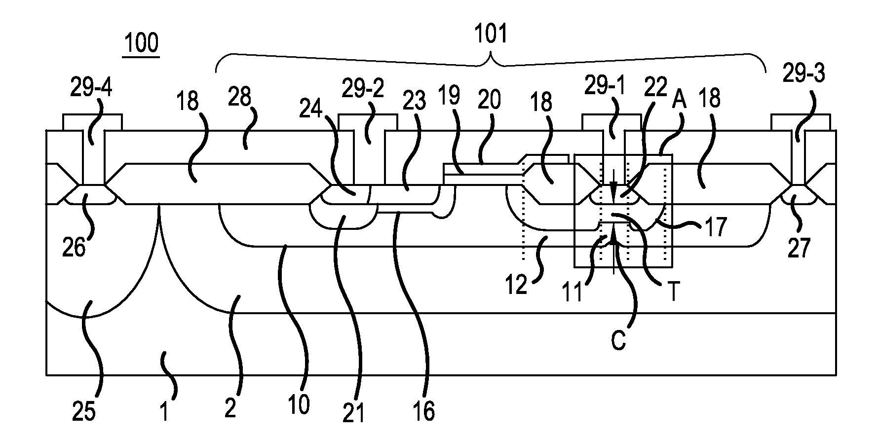
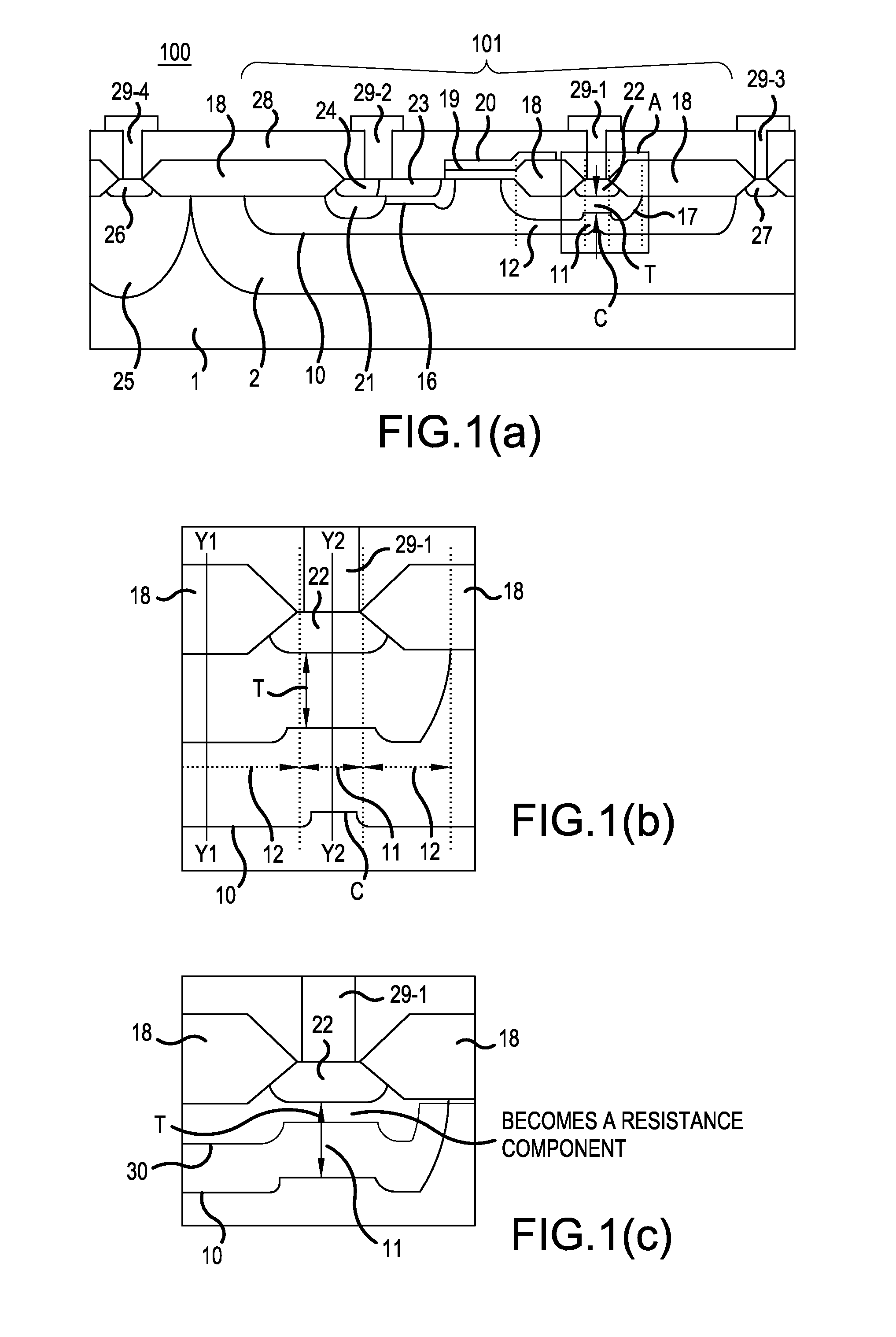
[0062]FIGS. 1A to 1C are diagrams illustrating semiconductor device 100 according to a first example of the invention, wherein FIG. 1A is a main portion sectional view, FIG. 1B is an enlargement of an A portion of FIG. 1A, and FIG. 1C is a diagram showing a depletion layer spreading inside second n-type offset layer 17. Semiconductor device 100 has n-type channel MOSFET 101 of a triple well structure (configured of first p-type well layer 25, n-type well layer 2, and second p-type well layer 10).

[0063]N-type channel MOSFET 101 configuring semiconductor device 100 includes a first p-type well layer (not shown) and n-type well layer 2 disposed in a surface layer of p-type semiconductor substrate 1, and second p-type well layer 10 formed by diffusion in a surface layer of n-type well layer 2. N-type channel MOSFET 101 includes n-type contact layer 27 formed by diffusion in a surface layer of n-type well layer 2. First p-type well layer 25 is a region for applying potential to p-type se...

example 2

[0083]FIGS. 4A to 6H are main portion manufacturing step sectional views of semiconductor device 100 manufacturing method, shown in step order, according to a second example of the invention. Herein, a description will be given of a method of manufacturing n-type channel MOSFET 101 configuring semiconductor device 100.

[0084]In FIG. 4A, n-type well layer 2 and the not shown first p-type well layer 25 are formed on the p-type semiconductor substrate 1. Second p-type well layer 10 is formed as a back gate region on n-type well layer 2. Also, there is a case in which n-type well layer 2 and first p-type well layer 25 are both formed by diffusion, and a case in which one of the wells is formed as an epitaxial layer. For example, when forming n-type well layer 2 as an epitaxial layer, an n-type epitaxial layer is formed on p-type semiconductor substrate 1, after which first p-type well layer 25 is formed by diffusion to a depth from the surface of the n-type epitaxial layer reaching p-typ...


PUM


Abstract

A semiconductor device and manufacturing method are disclosed which provide increased ESD resistance. By disposing a slit mask when forming a second p-type well layer, impurity concentration of the second p-type well layer is partially reduced. By forming a second n-type offset layer in the second p-type well layer having decreased impurity concentration, it is possible to increase thickness of the second n-type offset layer in this place compared with that heretofore known. By increasing thickness of the second n-type offset layer, a depletion layer does not reach an n-type drain layer at a low voltage when reverse bias is applied to the drain. It thus is possible to prevent thermal destruction caused by localized electrical field concentration. As a result, it is possible to increase ESD resistance. As it is sufficient to replace a photoresist mask, there is no increase in the number of processes.

Description

BACKGROUND OF THE INVENTION[0001]A. Field of the Invention[0002]The present invention relates to a semiconductor device and manufacturing method applied to, for example, a drive circuit having a floating potential as a reference.[0003]B. Description of the Related Art[0004]Power devices such as insulated gate bipolar transistors (IGBT) or power metal-oxide-semiconductor field-effect transistors (MOSFET) are utilized in many fields, such as motor controlling inverters, plasma display panels (PDP), power supply applications for flat panel displays (FPD) such as liquid crystal panels, and inverters for household electrical appliances such as air conditioners and lighting.[0005]To date, an electronic circuit configured by combining semiconductor devices such as a photocoupler and electronic parts such as a transformer has been used for the drive and control of these power devices. In recent years, however, high breakdown voltage ICs of breakdown voltage classes from 200V to 1,200V used ...

Claims


Application Information

Patent Timeline
IPC IPC(8): H01L29/06H01L29/66H01L29/78
CPCH01L29/0646H01L29/78H01L29/66477H01L21/266H01L29/66659H01L21/761H01L29/7835H01L29/0619H01L29/0649H01L29/0847H01L27/027
Inventor YAMAJI, MASAHARU
Owner FUJI ELECTRIC CO LTD
Why Eureka
Try Eureka