

Single Target Sputtering of Copper Zinc Tin Sulfide Selenide, CZT(S, Se)
a technology of copper zinc tin sulfide selenide and single target, which is applied in vacuum evaporation coating, sputtering coating, coating, etc., can solve the problems of inability to achieve co-evaporation, and ultimately limited energy production capacity of inorganic photovoltaic materials
- Summary
- Abstract
- Description
- Claims
- Application Information
AI Technical Summary
Benefits of technology
Problems solved by technology
Method used
Image

Examples
example
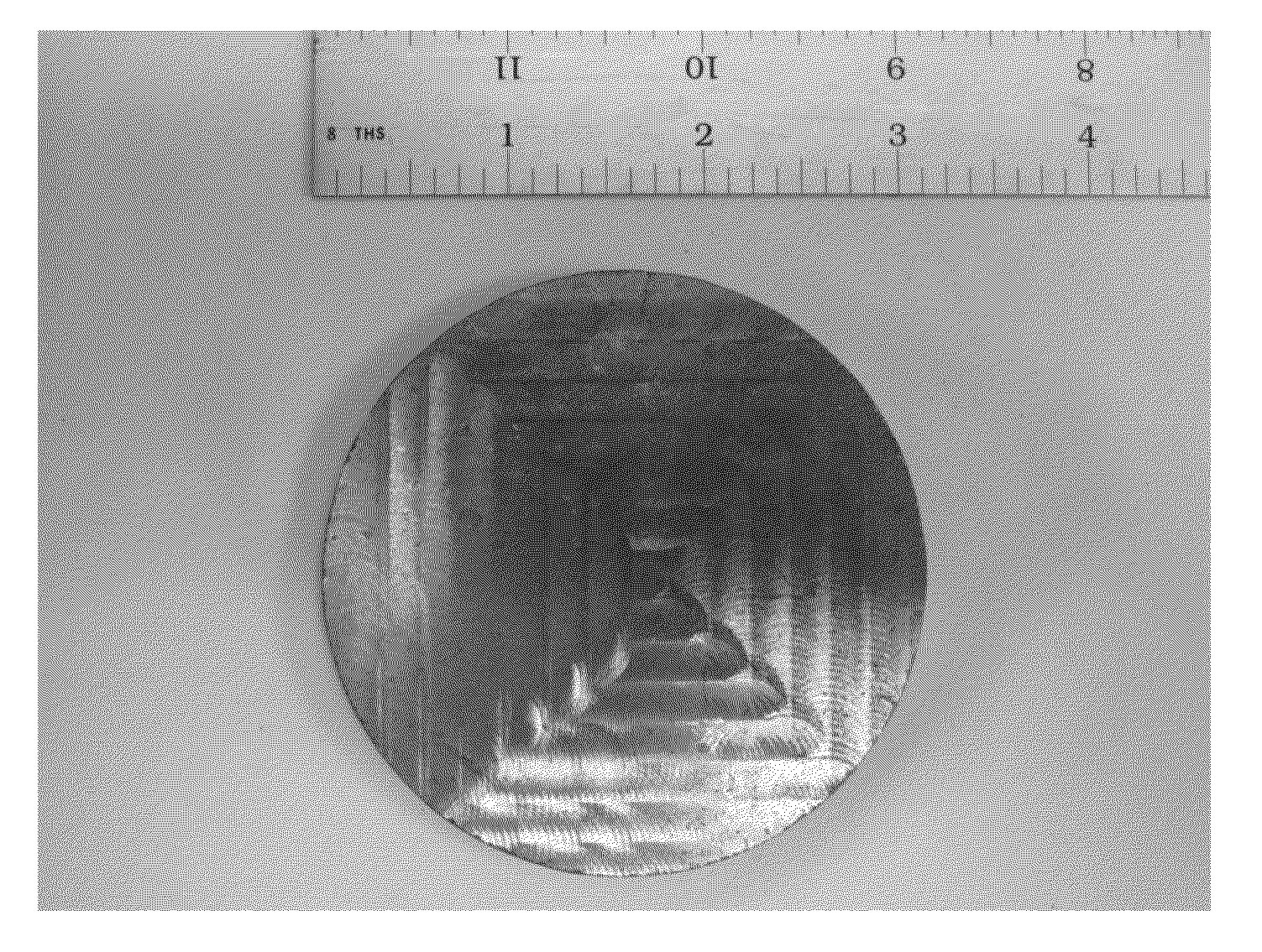
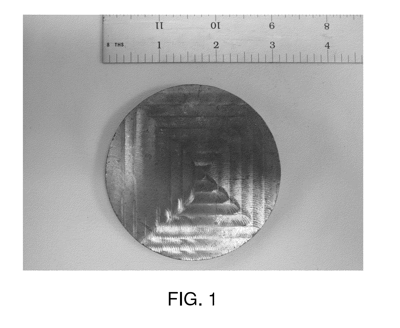
[0023]Elemental copper, zinc, tin and selenium were combined in a 2:1:1:4 molar ratio and sealed inside a quartz ampoule. The ampoule was then heated gradually to 750° C. and held at temperature for 30 hours to form CZTSe. The ampoule was then broken and the CZTSe is ground to a fine powder using a mortar and pestle. The powder was then placed in a hot press for one hour at 650° C. with a 10-ton ram force to form a compressed target that was subsequently machined to 3″ diameter by ⅛″ thick as seen in FIG. 1. A ruler measured in inches (2.54 cm) is also shown for scale). The target was indium-bonded to a copper backing plate prior to installation in a sputter deposition system.
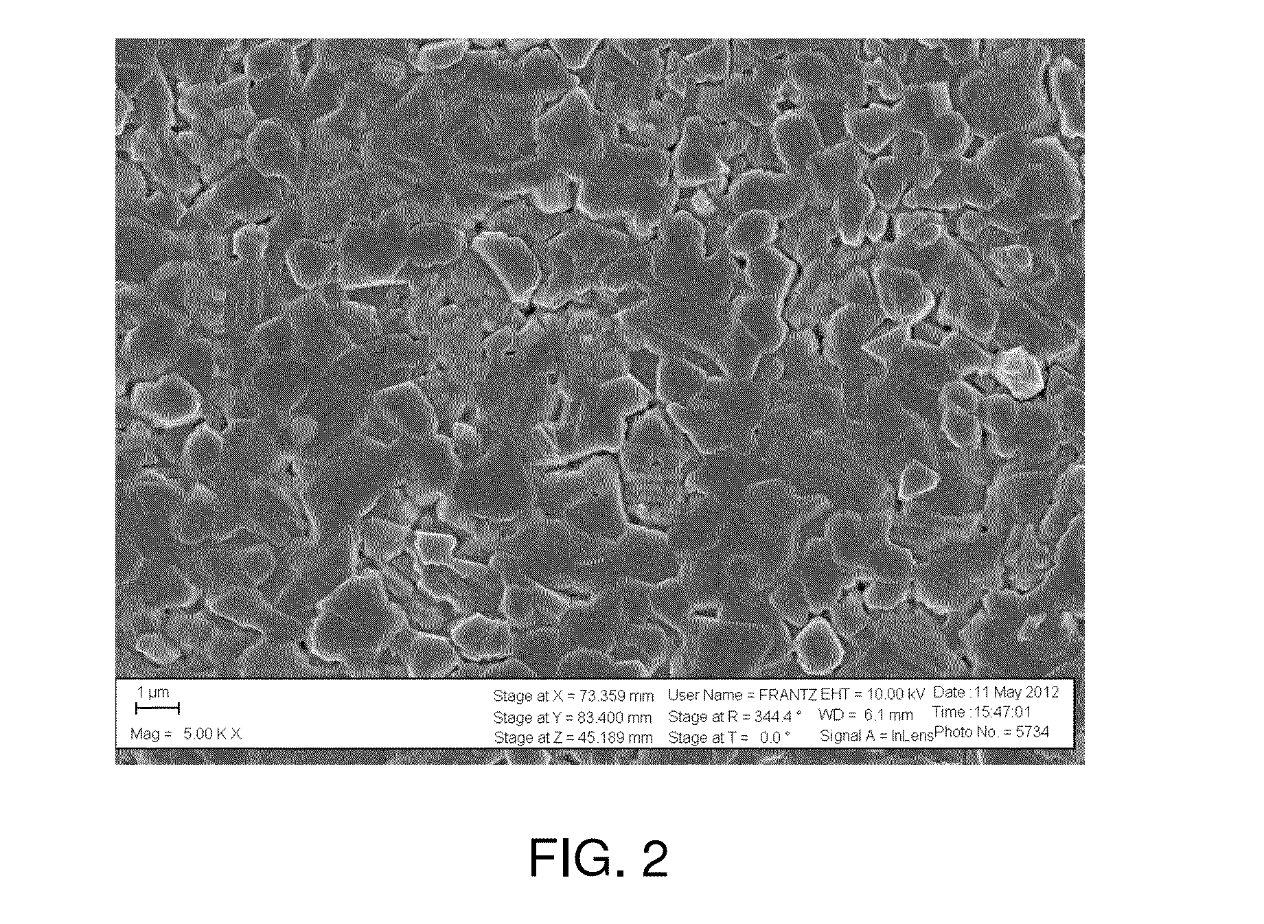
[0024]To form films, deposition was carried out onto a molybdenum-coated soda lime glass substrate, where the molybdenum served as the bottom electrode (anode) of the photovoltaic device. CZTSe was deposited onto the substrate using RF magnetron sputtering in a sputter-up geometry in an Ar atmosphere at a press...
PUM
| Property | Measurement | Unit |
|---|---|---|
| band gap | aaaaa | aaaaa |
| band gap | aaaaa | aaaaa |
| temperature | aaaaa | aaaaa |
Abstract
Description
Claims
Application Information