Semiconductor device and manufacturing method thereof

Active Publication Date: 2014-09-18
SEMICON ENERGY LAB CO LTD
View PDF2 Cites 14 Cited by
  • Summary
  • Abstract
  • Description
  • Claims
  • Application Information

AI Technical Summary

Benefits of technology

[0023]With the above structure, a miniaturized transistor having high electrical characteristics can be provided in a high yield.
[0024]Further, with t

Problems solved by technology

However, it is concerned that a yield of transistors in the manufacturing process is decreased due to miniaturization thereof.
For example, when an oxide semiconductor film which serves as a channel is microfabricated to have an island shape, unevenness

Method used


Image

  • Semiconductor device and manufacturing method thereof
  • Semiconductor device and manufacturing method thereof
  • Semiconductor device and manufacturing method thereof

Examples


Example

Embodiment 1

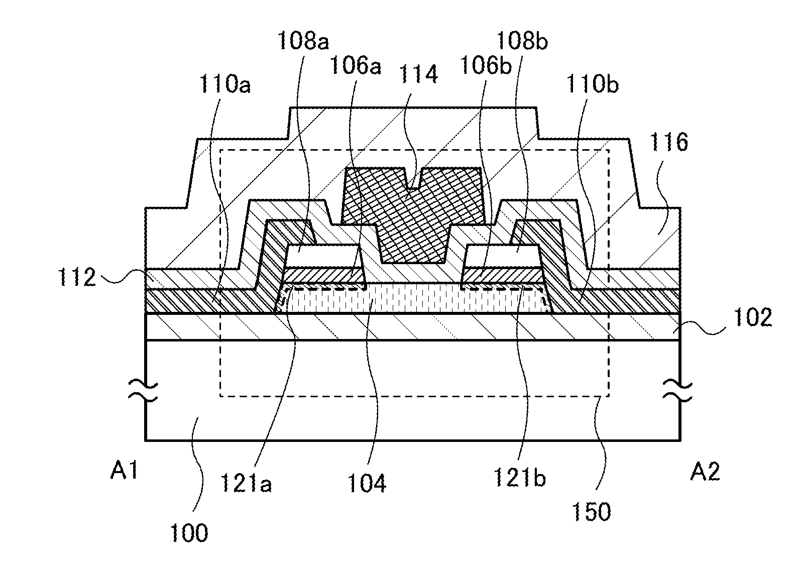
[0044]In this embodiment, a transistor which is a semiconductor device of one embodiment of the present invention is described with reference to drawings.

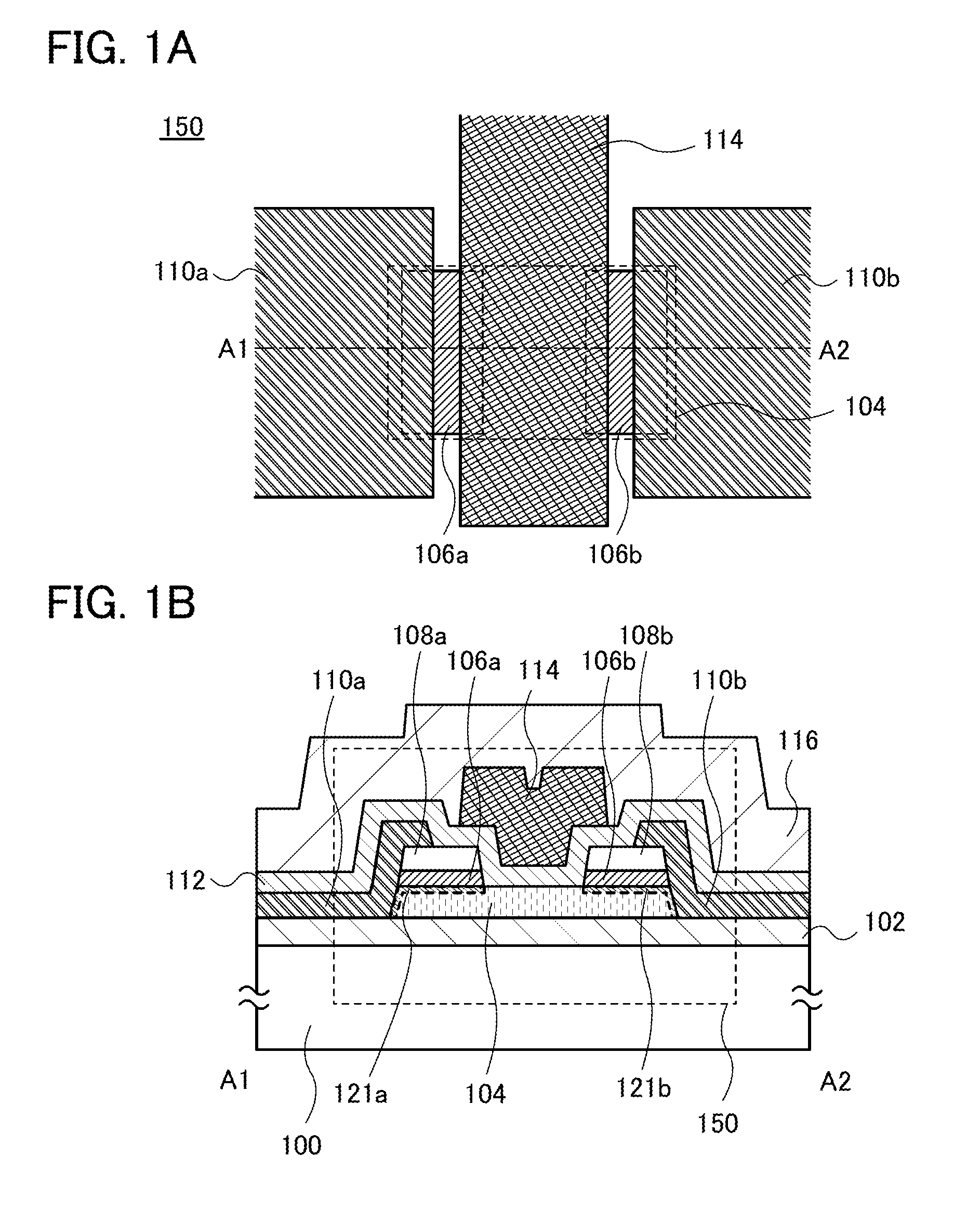
[0045]FIGS. 1A and 1B are a top view and a cross-sectional view of a transistor 150 of one embodiment of the present invention. FIG. 1A is the top view, and a cross section taken along a dashed-dotted line A1-A2 in FIG. 1A is illustrated in FIG. 1B. Note that for simplification of the drawing, some components in the top view in FIG. 1A are not illustrated.

[0046]The transistor 150 in FIGS. 1A and 1B includes a base insulating film 102 over a substrate 100; an oxide semiconductor film 104 over the base insulating film 102; a hard mask 106a and a hard mask 106b over the oxide semiconductor film 104; a hard mask 108a over the hard mask 106a; a hard mask 108b over the hard mask 106b; a source electrode 110a over the base insulating film 102, the oxide semiconductor film 104, and the hard masks 106a and 108a; a drain electrod...

Example

Embodiment 2

[0143]In this embodiment, a manufacturing method different from that of the transistor described in Embodiment 1 is described with reference to drawings.

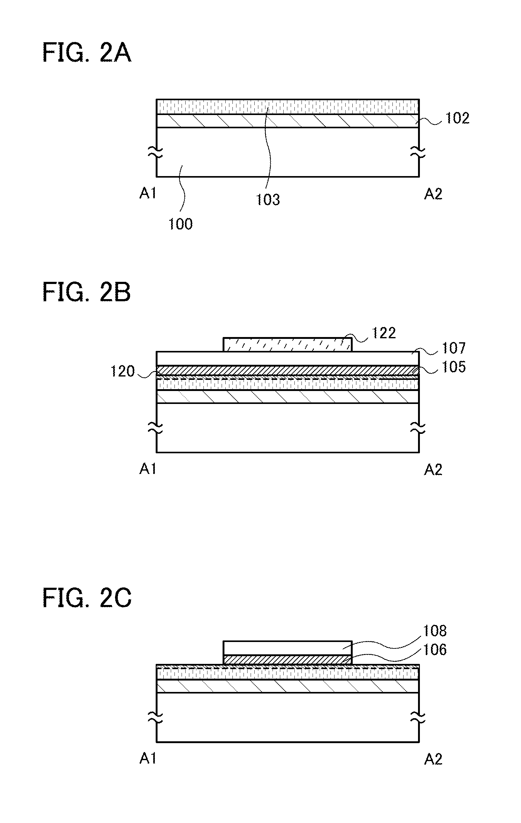
[0144]As in Embodiment 1, through the steps shown in FIGS. 2A to 2C and FIG. 3A, the base insulating film 102, the oxide semiconductor film 104, the low-resistance region 120a, the hard mask 106, and the hard mask 108 are formed over the substrate 100 (see FIG. 5A).

[0145]Next, a resist is formed over the base insulating film 102, the oxide semiconductor film 104, the hard mask 106, and the hard mask 108. Then, the resist is exposed to an electron beam, so that the resist mask 124 is formed (see FIG. 5B).

[0146]Instead of exposure using an electron beam, liquid immersion exposure in which ArF excimer laser light is used as a light source or EUV exposure may be used.

[0147]Next, the hard masks 106 and 108 are selectively etched using the resist mask 124 as a mask to form the hard masks 106a, 106b, 108a, and 108b (see FIG. 5C...

Example

Embodiment 3

[0161]In this embodiment, a transistor having a structure different from that of the transistor described in Embodiment 1 is described.

[0162]FIGS. 7A and 7B are a top view and a cross-sectional view of a transistor 250 of one embodiment of the present invention. FIG. 7A is the top view, and a cross section taken along a dashed-dotted line A1-A2 in FIG. 7A is illustrated in FIG. 7B. FIG. 7C is an enlarged view of a region surrounded by a dashed-line circle in FIG. 7B. Note that for simplification of the drawing, some components in the top view in FIG. 7A are not illustrated.

[0163]The transistor 250 in FIGS. 7A to 7C includes the base insulating film 102 over the substrate 100; an oxide film 204a over the base insulating film 102; an oxide semiconductor film 204b over the oxide film 204a; an oxide film 204c over the oxide semiconductor film 204b; the hard masks 106a and 106b over the oxide film 204c; the hard mask 108a over the hard mask 106a; the hard mask 108b over the h...


PUM


Abstract

When an oxide semiconductor film is microfabricated, with the use of a hard mask, unevenness of a side surface of the oxide semiconductor film can be suppressed. Specifically, a semiconductor device comprises an oxide semiconductor film over an insulating surface; a first hard mask and a second hard mask over the oxide semiconductor film; a source electrode over the oxide semiconductor film and the first hard mask; a drain electrode over the oxide semiconductor film and the second hard mask; a gate insulating film over the source electrode and the drain electrode; and a gate electrode overlapping with the gate insulating film and the oxide semiconductor film, and the first and second hard masks have conductivity.

Description

BACKGROUND OF THE INVENTION[0001]1. Field of the Invention[0002]The present invention relates to a semiconductor device and a manufacturing method thereof.[0003]Note that in this specification, a semiconductor device refers to any device that can function by utilizing semiconductor characteristics, and an electro-optical device, a semiconductor circuit, and an electronic device are all included in the category of semiconductor devices.[0004]2. Description of the Related Art[0005]Transistors used for most flat panel displays typified by a liquid crystal display device or a light-emitting display device are formed using a silicon semiconductor such as amorphous silicon, single crystal silicon, or polycrystalline silicon provided over a glass substrate. Further, such a transistor employing such a silicon semiconductor is used in integrated circuits (ICs) and the like.[0006]In recent years, attention has been drawn to a technique in which, instead of a silicon semiconductor, a metal oxi...

Claims


Application Information

Patent Timeline
IPC IPC(8): H01L29/786H01L29/66
CPCH01L29/66969H01L29/7869H01L27/1288H01L29/41733H01L29/45H01L29/78696H01L27/1225H01L27/1259
Inventor SASAGAWA, SHINYAKURATA, MOTOMU
Owner SEMICON ENERGY LAB CO LTD
Why Eureka
Try Eureka