Graphene based field effect transistor

a graphene-based field effect transistor and transistor technology, applied in the field of graphene-based semiconductor devices, can solve problems such as particularly challenging, and achieve the effects of low leakage current, high capacitance, and efficient and uniform seeding ald growth

Active Publication Date: 2014-10-09
INTERUNIVERSITAIR MICRO ELECTRONICS CENT (IMEC VZW) +1
View PDF3 Cites 28 Cited by
  • Summary
  • Abstract
  • Description
  • Claims
  • Application Information

AI Technical Summary

Benefits of technology

[0005]A clear need remains the art for a graphene chemical functionalization that: (i) efficiently and uniformly seeds ALD growth; (ii) preserves the underlying graphene structure; and (iii) achieves desirable dielectric properties such as low leakage current and high capacitance. Good graphene-based semiconductor devices comprising an ALD-grown high-k dielectric layer are also desirable. This has been particularly challenging before due to the bad nucleation of ALD layers on the graphene surface.

Problems solved by technology

This has been particularly challenging before due to the bad nucleation of ALD layers on the graphene surface.

Method used


Image

  • Graphene based field effect transistor
  • Graphene based field effect transistor
  • Graphene based field effect transistor

Examples


example 1

Device Fabrication

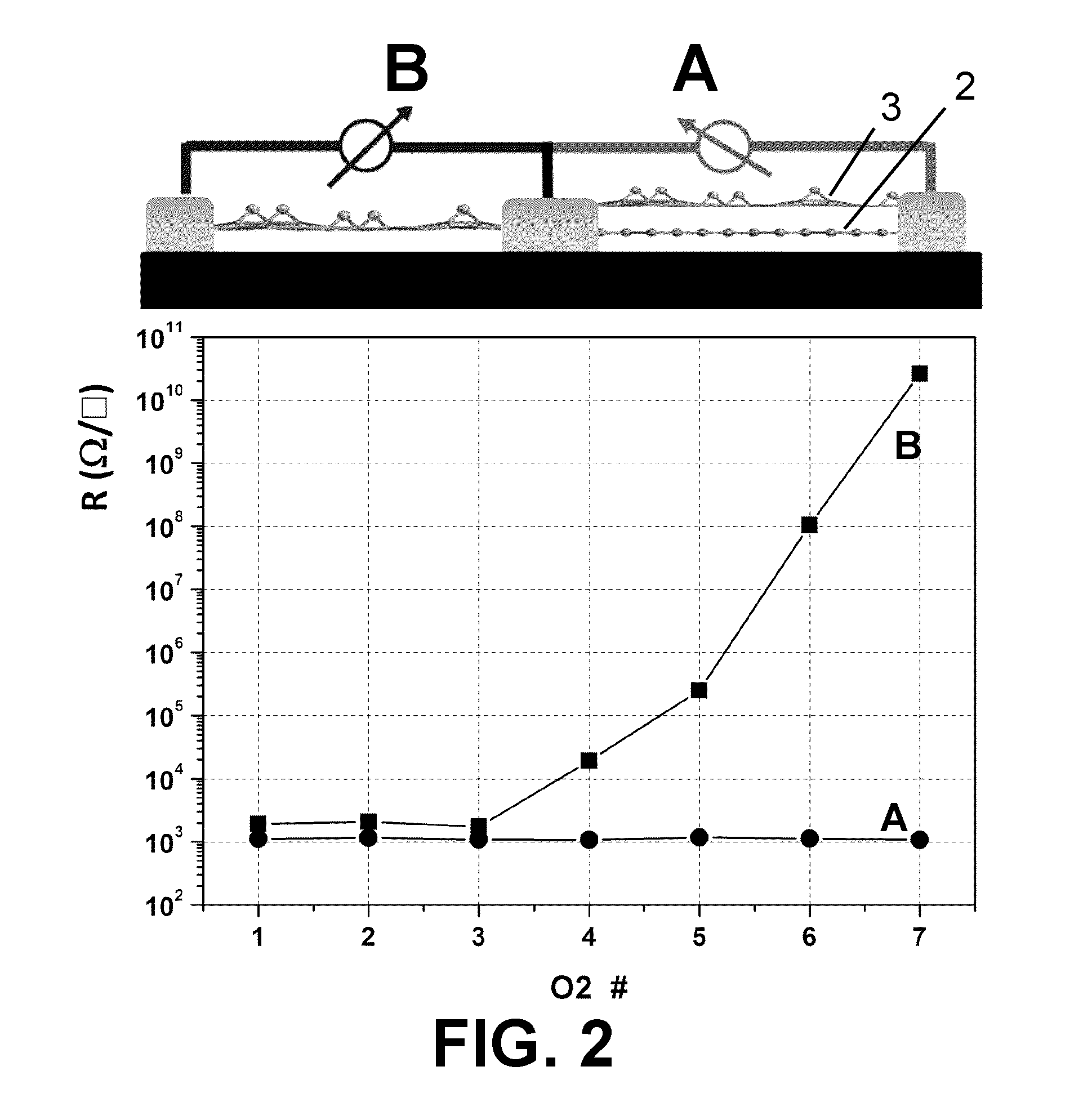
[0076]Reference is now made to FIG. 2.

[0077]Both samples A and B were formed on the same substrate (4).

[0078]Preparation of sample B:

[0079]A single layer graphene (SLG) flake (2) was deposited by micromechanical exfoliation on an n-doped Si substrate (4) covered with a 90 nm thermally grown SiO2 film, thereby forming sample B.

[0080]Preparation of sample A:

[0081]A single layer graphene (SLG) flake (2) was deposited by micromechanical exfoliation on an n-doped Si substrate (4) covered with a 90 nm thermally grown SiO2 film.

[0082]A large graphene film was then grown on copper thin film via Chemical Vapor Deposition (CVD). This film was then isolated from the copper foil and transferred onto the SiO2-supported graphene flake (2) by the standard polymethyl-methacrylate (PMMA) transferring method, thereby forming a substrate-double-layer graphene stack (sample A).

[0083]Standard photolithography was then performed on both sample A and sample B to (i) pattern samples A and...

example 2

Electrical Characterization

[0085]The resistances of samples A and B were measured after each plasma exposure / annealing step.

[0086]FIG. 2 compares the resistance of A and B versus the number of plasma exposure pulses.

[0087]The resistance of sample A was relatively constant while the resistance of sample B exponentially increased to 1011Ω.

[0088]Sample B (CVD graphene) changed to high resistance (insulator) upon oxidation.

[0089]The almost-constant resistance observed for sample A (stack of exfoliated single layer graphene (SLG) & CVD graphene) indicates that the underlying (metallic) SLG remains intact once the top layer (CVD graphene) undergoes oxidation.

[0090]We now refer to FIG. 3.

[0091]The most discussed feature in Raman spectra of graphene is the so-called 2D peak around 2700 cm−1, which is attributed to a two-phonon intervalley Raman scattering process. In the case of single layer graphene, the 2D peak consists of a single peak due to the presence of a single valence and conducta...

example 3

Top Date Stack Fabrication

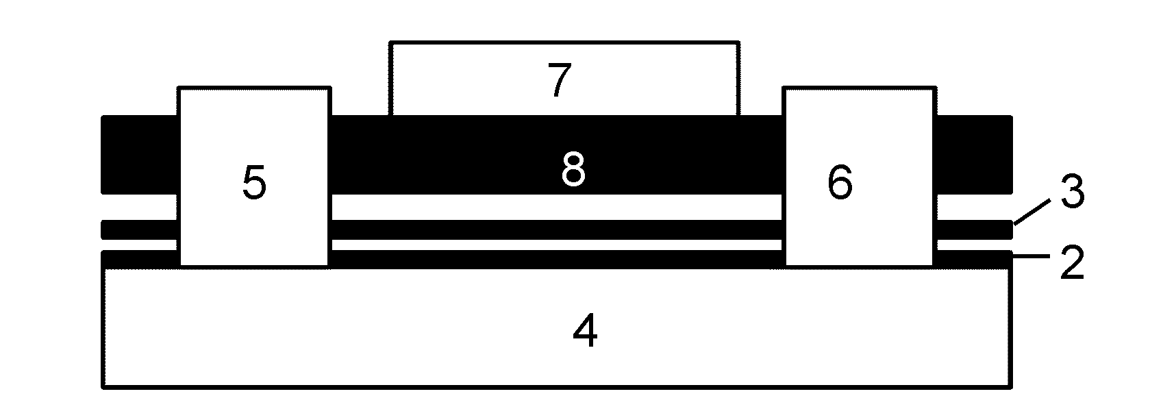
[0092]A 30 nm Al2O3 layer was deposited by ALD on the oxygen rich surface of sample 1 at 150° C. using alternate pulses of trimethylaluminum (TMA) and water. The dual-gate FET fabrication was then completed by fabricating a top-gate electrode by e-beam lithography (1 nm / 50 nm Cr / pd). FIG. 4 shows a schematic representation of a dual-gated FET with a graphene 2-graphene oxide 3 stack, wherein the graphene 2 is the channel and ALD-Al2O3 is grown on the graphene oxide 3.

[0093]FIG. 5 shows the transfer characteristics (Resistance R vs top-gate voltage (VTG)) of the dual-gated FET of example 3 at different voltages. It demonstrates that the source-drain resistance can be modulated with the device obtained in example 3.

[0094]FIG. 4 shows a Field effect transistor according to embodiments of the present disclosure. It comprises a semiconductor substrate 4 bearing a graphene layer 2 and a graphene oxide layer 3. It further comprises a high-k dielectric layer 8 on t...


PUM

PropertyMeasurementUnit
thicknessaaaaaaaaaa
thicknessaaaaaaaaaa
optical band gapaaaaaaaaaa

Abstract

A semiconductor device comprising a graphene layer, a graphene oxide layer overlaying the graphene layer, and a high-k dielectric layer overlaying the graphene oxide layer is provided, as well as a method for producing the same. The method results in a graphene chemical functionalization that efficiently and uniformly seeds ALD growth, preserves the underlying graphene structure, and achieves desirable dielectric properties such as low leakage current and high capacitance.

Description

INCORPORATION BY REFERENCE TO RELATED APPLICATION[0001]Any and all priority claims identified in the Application Data Sheet, or any correction thereto, are hereby incorporated by reference under 37 CFR 1.57. This application claims the benefit of European Application No. 13162837.2 filed Apr. 9, 2013. The aforementioned application is incorporated by reference herein in its entirety, and is hereby expressly made a part of this specification.TECHNICAL FIELD OF THE DISCLOSURE[0002]The present disclosure relates to the field of semiconductor devices and in particular to the field of graphene-based semiconductor devices. The present disclosure also relates to methods for the manufacture of such devices.BACKGROUND OF THE DISCLOSURE[0003]An important step in the development of top-gated graphene-based field-effect transistors (FETs) is the growth of high dielectric constant (high-k) materials to act as the gate insulator. For optimal performance, these dielectric thin films should be ultr...

Claims


Application Information

Patent Timeline
Patent Type & Authority Applications(United States)
IPC IPC(8): H01L29/775H01L29/16H01L21/02
CPCH01L29/775H01L21/02527H01L29/778H01L29/1606H01L29/513H01L21/0262H01L2924/13088H01L29/66015
Inventor NOURBAKHSH, AMIRHASANHEYNS, MARCDE GENDT, STEFAN
Owner INTERUNIVERSITAIR MICRO ELECTRONICS CENT (IMEC VZW)
Why Eureka
Try Eureka