Eureka AIR delivers breakthrough ideas for toughest innovation challenges, trusted by R&D personnel around the world.

Method of making a transitor

Inactive Publication Date: 2014-12-18
COMMISSARIAT A LENERGIE ATOMIQUE ET AUX ENERGIES ALTERNATIVES +2
View PDF6 Cites 6 Cited by
  • Summary
  • Abstract
  • Description
  • Claims
  • Application Information

AI Technical Summary

Benefits of technology

The present invention is suitable for preserving the thickness of an initial insulating layer on semiconductor on insulator substrates, such as silicon on insulator, without the need for etching the initial BOX layer to obtain a buried source and drain. This invention is compatible with substrates that integrate a thin or thick BOX layer. The technical effect is the improvement of the manufacturing process of MOSFET transistors where an initial cavity is formed in the semiconductor layer without the need for etching the initial BOX layer.

Problems solved by technology

Replacing the nitride does however significantly complicate the standard method for manufacturing MOSFET transistors.
This material does however lend itself much less well than nitride to the production of spacers and there does not currently exist any industrially reliable method that allows direct replacement of nitride.
This so-called “faceted epitaxy” technique is however particularly difficult to master.
Thus there are disparities in thickness between wide and narrow devices that may cause malfunctioning such as total siliconising and the appearance of leakage current that serious impairs the reliability of the devices.
From this brief presentation of the known methods for producing MOSFET transistors, it is clear that there do not exist any simple and reliable methods that make it possible to reduce both the access resistance of the source and drain electrodes and the stray capacitance between these electrodes and the control gate.

Method used


Image

  • Method of making a transitor
  • Method of making a transitor
  • Method of making a transitor

Examples


first embodiment

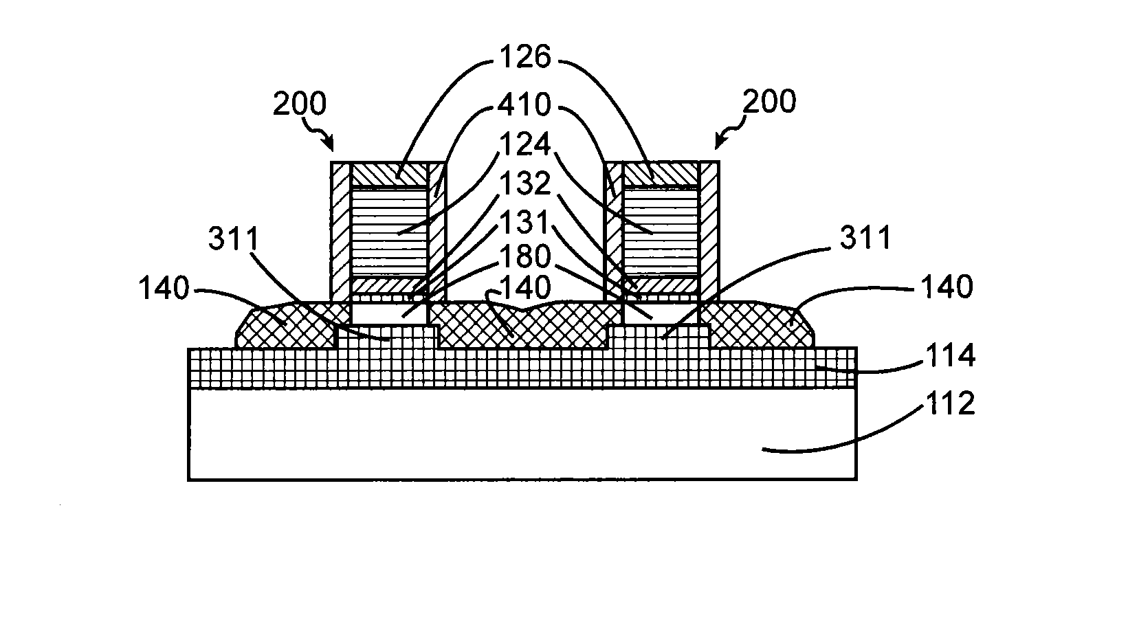
[0056] said etching of at least the additional layer of semiconductor material removes, on either side of the gate stack, the entire thickness of the additional layer of semiconductor material and the entire thickness of the initial semiconductor layer. Preferably, the etching is stopped on the insulating layer. Thus the etching bares the insulating layer on either side of the gate stack. The formation of the source and drain is effected by epitaxy from the semiconductor material remaining in place. This epitaxy is preferentially directed downwards, that is to say from the channel and in the direction of the substrate.

second embodiment

[0057]In a second embodiment, said etching preserves, on either side of the gate stack, a film formed by at least a portion of the thickness of the initial semiconductor layer and optionally by a portion of the additional layer of semiconductor material. Thus the etching is partial in that it does not bare the insulating layer on either side of the gate stack. Advantageously, in this case, the epitaxy is initiated by the lateral ends of the channel and / or by the film of semiconductor material left in place, on either side of the gate stack, on the insulating layer at the end of the etching. Typically only a top portion of the assembly formed by the additional layer of semiconductor material and the initial semiconductor layer is removed. Said top portion removed by anisotropic etching typically has a thickness of between 1 nm and 20 nm.

[0058]According to a first embodiment, the formation of at least one cavity is effected by etching only part of the thickness of the initial semicond...


PUM


Abstract

The invention relates to a method for manufacturing a transistor comprising the preparation of a stack of layers of the semiconductor on insulator type comprising at least one substrate on which an insulating layer and an initial semiconductor layer are successively disposed. The method includes the formation of at least one oxide pad extending from a top face of the insulating layer, the formation of an additional layer made from semiconductor material covering the oxide pad and intended to form a channel for the transistor, the formation of a gate stack above the oxide pad, and the formation of a source and drain on either side of the gate stack.

Description

TECHNICAL FIELD OF THE INVENTION[0001]The present invention concerns in general transistors of the metal oxide semiconductor field effect (MOSFET) type and more particularly the reduction of parasitic elements limiting the operating speed thereof.PRIOR ART[0002]In a MOSFET transistor a current is made to flow between a “source” electrode and a “drain” electrode under the control of a control “gate”, which creates a conduction channel between source and drain as soon as a sufficient voltage is applied thereto. The maximum switching speed of a MOSFET transistor depends on the speed with which it is possible to effectively establish the conduction current and make it disappear. It depends among other things on many physical parameters particular to the materials used, such as for example the mobility of the carriers of the semiconductor material used and the levels and type of doping of the various regions defining the electrodes. The switching speed also depends largely on the geometr...

Claims


Application Information

Patent Timeline
IPC IPC(8): H01L29/66H01L21/02
CPCH01L29/66772H01L29/66636H01L21/02667H01L21/84H01L29/78603H01L21/76205H01L21/76248H01L21/02532H01L21/02538H01L21/02645H01L21/28123H01L21/7624
Inventor NIEBOJEWSKI, HEIMANUMORAND, YVESVINET, MAUD
Owner COMMISSARIAT A LENERGIE ATOMIQUE ET AUX ENERGIES ALTERNATIVES
Why Eureka
Eureka Blog
Learn More