

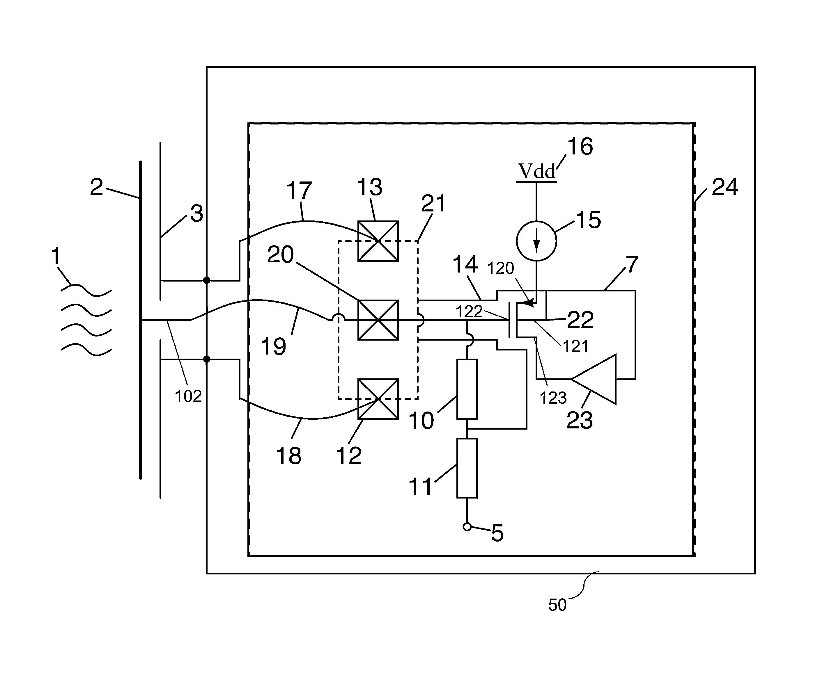
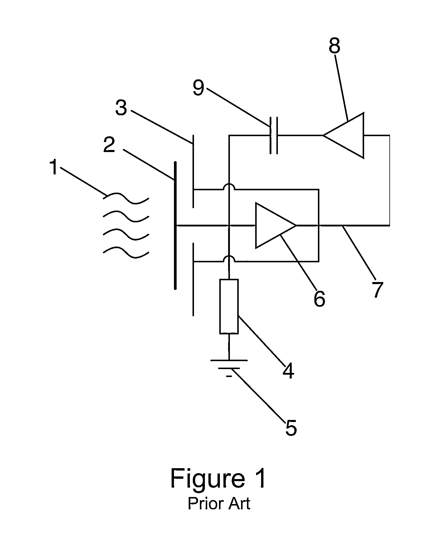
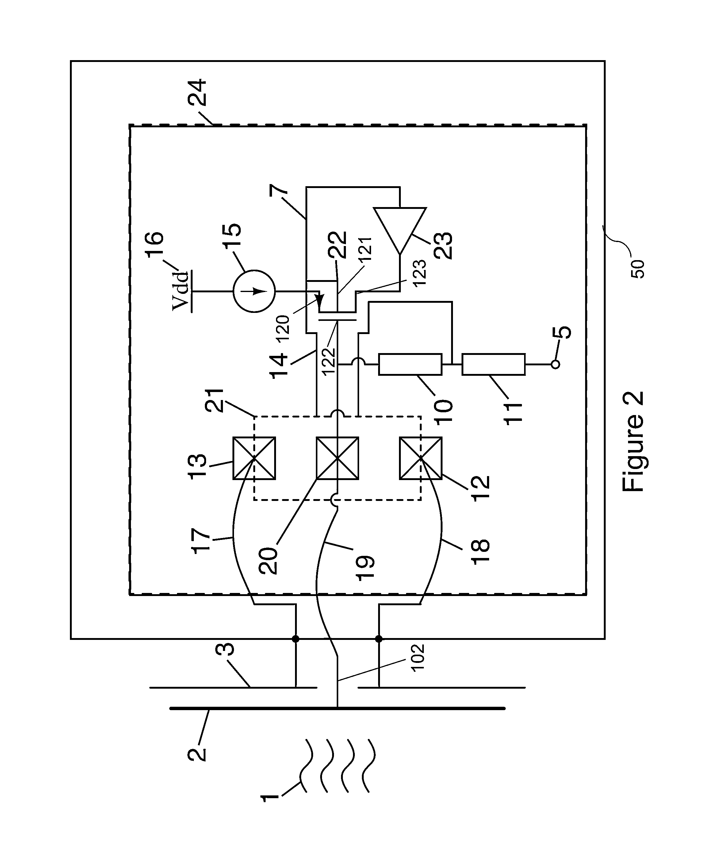
Integrated electric field sensor
a technology of integrated electric field and sensor, which is applied in the direction of resistance/reactance/impedence, electrostatic field measurement, instruments, etc., can solve the problems of reducing the efficiency of reducing the internal capacitance of a discrete amplifier, reducing the efficiency of implementing a high impedance amplifier using discrete components (e.g., transistors, resistors, capacitors) with bootstrapping, and reducing noise. , the effect of reducing the nois
- Summary
- Abstract
- Description
- Claims
- Application Information
AI Technical Summary
Benefits of technology
Problems solved by technology
Method used
Image

Examples
example 1
Data Acquisition System and ECG Measurement
[0049]A wireless bioinstrumentation platform capable of supporting various electrodes was designed around the TEXAS INSTRUMENTS TI ADS 1298, which provides an array of eight 24-bit A / D converters. The high resolution of the ADS1298 allows for the use of minimal voltage gain (0dB-6 dB) and a fully DC-coupled signal path, which makes the system immune to DC offset errors and long overload recovery times from high-pass filters. The device provides connectors and power to support up to four active electrodes. An additional four passive electrodes can also be included.
[0050]A PIC24 microcontroller (Microchip Technology, Inc., Chandler, Ariz.) is used to interface the ADS 1298 with the BLUETOOTH® module. Data is streamed to a PC or other appropriate processing system from the device at a rate of 500 sps via a standard BLUETOOTH® serial port interface. The fully wireless device minimizes the influence of power line interference to ensure low noise...
example 2
EEG Signal Validation
[0054]The same sensor used in Example 1 was used to validate its application to EEG BCI (brain-computer interface) and monitoring. A simple alpha wave experiment was used. Spectrograms of EEG data were taken during a trial where a subject was asked to close their eyes from the segment spanning 5 to 20 seconds into the trial. The integrated sensor was able to resolve alpha waves through hair over the occipital region. The presence and absence of alpha activity was confirmed by an Ag / AgCl control electrode placed on the forehead.
[0055]Steady-state visual evoked potential experiments are effective at verifying the performance of EEG sensor systems since it relies on detecting known and controlled narrowband stimuli. In addition, it also serves as a common BCI paradigm. For the experiment, the integrated amplifier electrode was mounted in a relatively loose-fitting headband over the occipital region. A second Ag / AgCl electrode was placed on the forehead and used as ...
PUM
 Abstract
Description
Claims
Application Information