Transmit/Receive Daughter Card With Integral Circulator

Active Publication Date: 2015-01-15
RAYTHEON CO
View PDF0 Cites 93 Cited by
  • Summary
  • Abstract
  • Description
  • Claims
  • Application Information

AI Technical Summary

Benefits of technology

[0046]With this particular arrangement, a tile sub-array can be manufactured without the need to perform any back-drill and back-fill operations typically required to eliminate RF via stubs. The RF matching pad technique refers to a technique in which a conductor is provided on blank layers (i.e., layers with no copper) of a circuit board or in ground plane layers (with etched relief area) of a circuit board. The conductor and associated relief area provided the mechanism to adjust impedance characteristics of RF vias (also referred to as RF interconnect circuits) provided in a circuit board. Since the need to utilize back-drill and back-fill operations is eliminated, the RF matching pad approach enables a standard, low aspect ratio drill and plate manufacturing operation to produce an RF via that connects inner circuit layers and which also has a low insertion loss characteristic acros

Problems solved by technology

At the same time, bandwidth, polarization diversity and reliability requirements of such systems become increasingly more difficult to meet.
This step improves RF performance of the PWB but increases cost and degrades RF performance due to back-drill tolerances, back-fill material dielectric properties and trapped air pockets.
Thus, this approach results in high cost RF multilayer PWB laminates due to multiple fabrication operations and back-drill/backfill operations.
Mixed signal multilayer PWBs provided using low temperature co-fired ceramic (LTCC) based materials (rather than PTFE-based materials) present a different set of fabrication problems.
For example, processing can only be done on relatively small panel (or board) sizes (typically 6″ square or less) due to shrinkage issues.
Also, LTCC based materials use a conductive paste for transmission lines and ground planes and such conductive paste is lossy at RF frequencies compared to losses in RF signals propagating through pure copper transmission lines used in PTFE boards.
Such increased insertion loss is unacceptable at many frequency ranges (e.g. at Ku-Band and above).
Furthermore, LTCC materials

Method used


Image

  • Transmit/Receive Daughter Card With Integral Circulator
  • Transmit/Receive Daughter Card With Integral Circulator
  • Transmit/Receive Daughter Card With Integral Circulator

Examples


Embodiment Construction

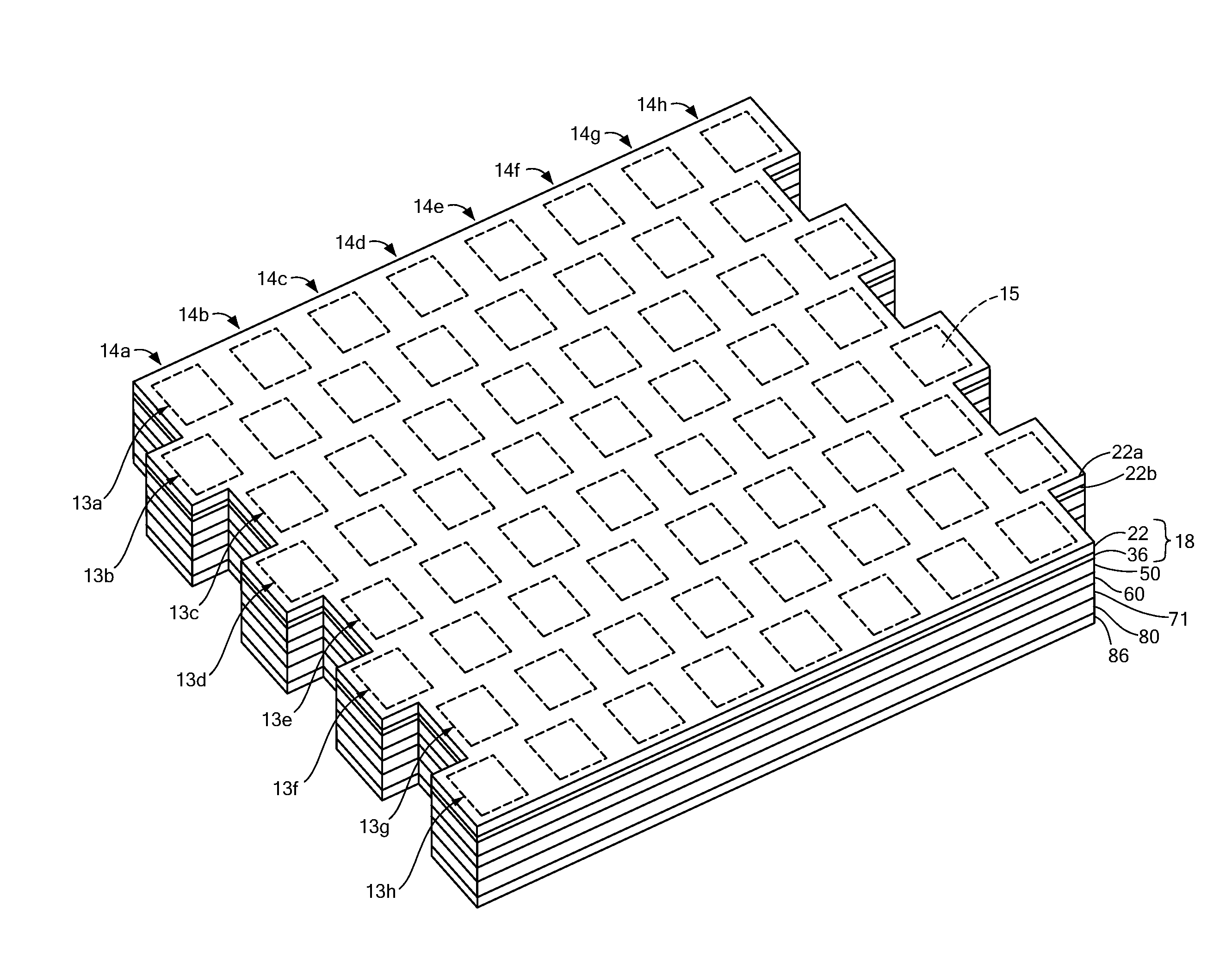
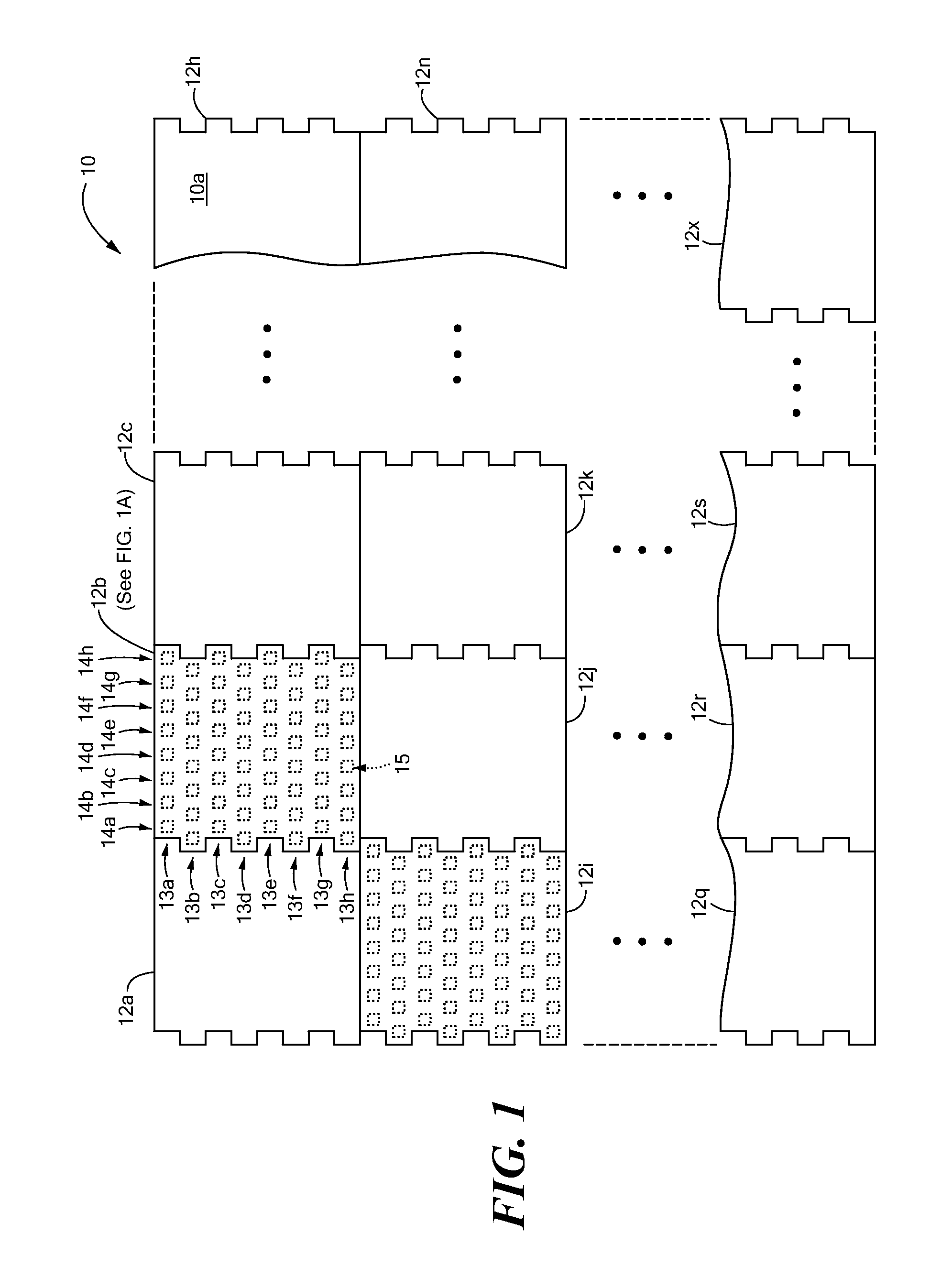
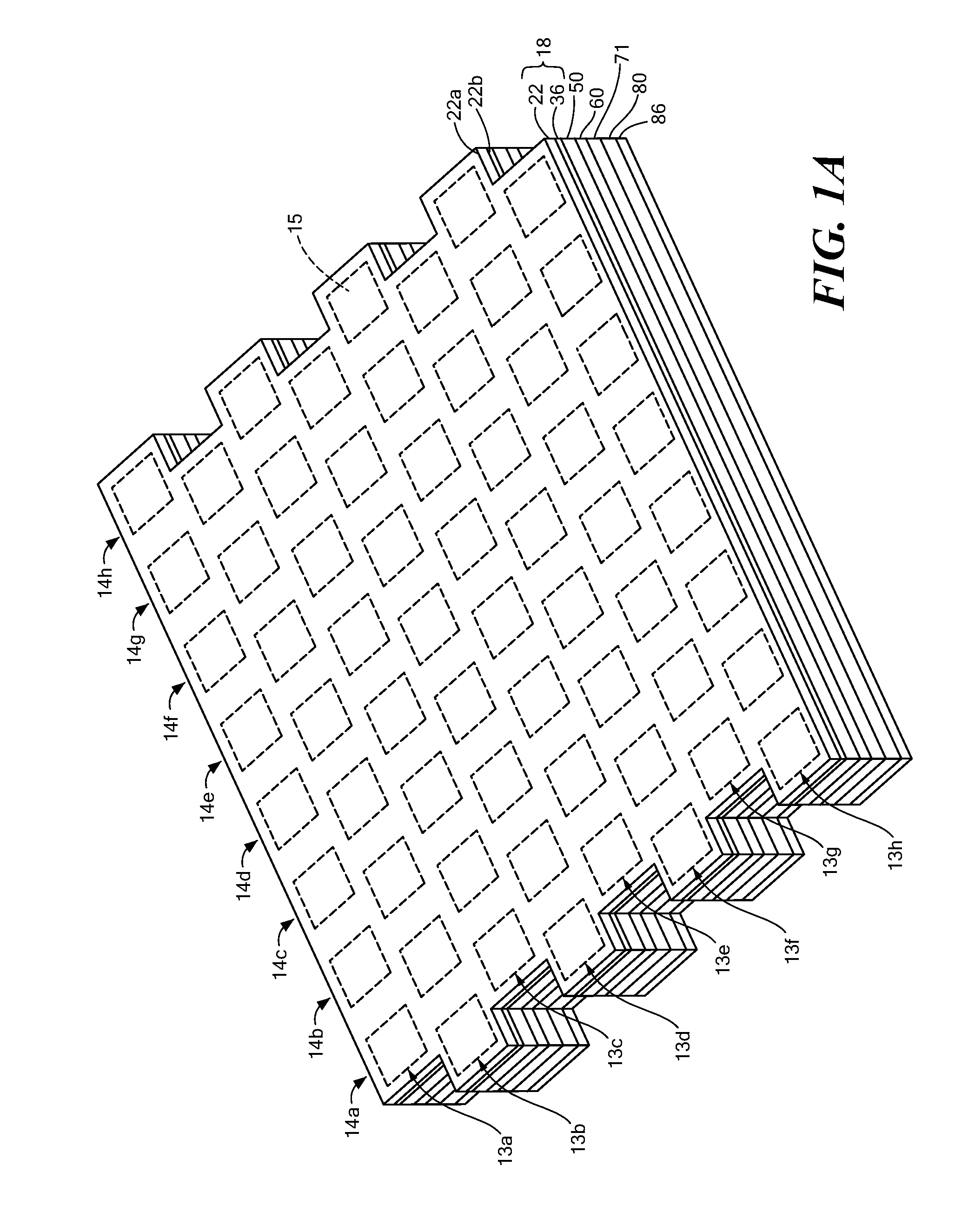
[0088]Before describing the various embodiments of the invention, some introductory concepts and terminology are explained. A “panel array” (or more simply “panel) refers to a multilayer printed wiring board (PWB) which includes an array of antenna elements (or more simply “radiating elements” or “radiators”), as well as RF, logic and DC distribution circuits in one highly integrated PWB. A panel is also sometimes referred to herein as a tile array (or more simply, a “tile”).

[0089]An array antenna may be provided from a single panel (or tile) or from a plurality of panels. In the case where an array antenna is provided from a plurality of panels, a single one of the plurality of panels is sometimes referred to herein as a “panel sub-array” (or a “tile sub-array”).

[0090]Reference is sometimes made herein to an array antenna having a particular number of panels. It should of course, be appreciated that an array antenna may be comprised of any number of panels and that one of ordinary ...


PUM


Abstract

A mixed-signal, multilayer printed wiring board fabricated in a single lamination step is described. The PWB includes one or more radio frequency (RF) interconnects between different circuit layers on different circuit boards which make up the PWB. The PWB includes a number of unit cells with radiating elements and an RF cage disposed around each unit cell to isolate the unit cell. A plurality of flip-chip circuits are disposed on an external surface of the PWB and a heat sink can be disposed over the flip chip components.

Description

CROSS-REFERENCE TO RELATED APPLICATIONS[0001]This patent application is a continuation-in-part of co-pending application Ser. No. 13 / 295,437 filed Nov. 14, 2011 entitled: An Active Electronically Scanned Array (AESA) Card which is a continuation-in-part of application Ser. No. 12 / 484,626, filed Jun. 15, 2009 now U.S. Pat. No. 8,279,131 entitled “PANEL ARRAY,” which application claims the benefit, under 35 U.S.C. §119 (e), of U.S. Provisional Application No. 61 / 1163,002 (RTN-411PUSP) filed Mar. 24, 2009, now abandoned.[0002]This patent application is also a continuation-in-part of co-pending application Ser. No. 12 / 694,450 filed Jan. 27, 2010 entitled: “Radio Frequency Interconnect Circuits and Techniques” which is a divisional of U.S. patent application Ser. No. 11 / 558,126 filed on Nov. 9, 2006 now U.S. Pat. No. 7,671,696 entitled: “Radio Frequency Interconnect Circuits and Techniques” issued on Mar. 2, 2010 which is a continuation of U.S. patent application Ser. No. 11 / 533,848 (RTN...

Claims


Application Information

Patent Timeline
IPC IPC(8): H01Q21/00H05K1/02H01P1/38
CPCH01P1/38H01Q21/0025H05K1/0207H05K1/0206H01L2223/6677H01L2223/6683H01L2224/16227H01L2224/73253H01Q1/02H01Q9/0414H01Q21/00H01Q21/0087H01Q21/065
Inventor PUZELLA, ANGELO M.BOZZA, DONALD A.ROBBINS, JAMES R.FRANCIS, JOHN B.
Owner RAYTHEON CO
Why Eureka
Try Eureka