

Conductive Hard Carbon Film and Method for Forming the Same
a technology of conductive hard carbon film, which is applied in the direction of conductors, natural mineral layered products, instruments, etc., can solve the problems of inability to ensure stable quality, increased costs, and decreased productivity, and achieves high hardness and stable volume resistivity and hardness
- Summary
- Abstract
- Description
- Claims
- Application Information
AI Technical Summary
Benefits of technology
Problems solved by technology
Method used
Image

Examples
example 1
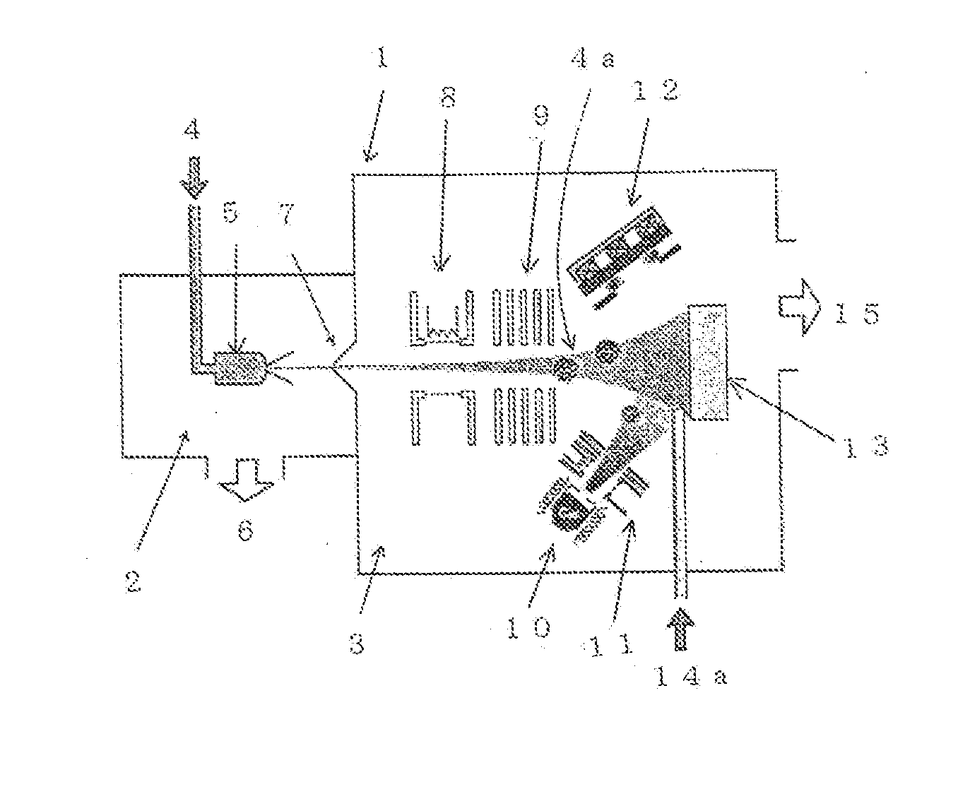
[0087]A 50 mm×50 mm square silicon wafer was used as the base material (13). This silicon wafer was set in the apparatus shown in FIG. 1 and irradiated, for purification of the surface of the silicon wafer, with argon cluster ions at 5×10¹⁶ clusters / cm2, the cluster ions having the average argon atom number of 1000 and being accelerated at 20 kV. The number of argon atoms composing one cluster was measured by the time-of-flight method. The argon cluster ions were generated using the cluster generation nozzle (5) made of glass, introduced to the processing unit using gas cluster ions (3) through the skimmer (7), and ionized by electron impact in the ionization unit (8) so as to collide against the surface of the silicon wafer (13).
[0088]After the surface of the silicon wafer was purified, fullerene was evaporated in a crucible to give evaporated particles of a carbonaceous material and at the same time 0.1 sccm of evaporated particles of diborane was supplied as the evaporated partic...
example 2
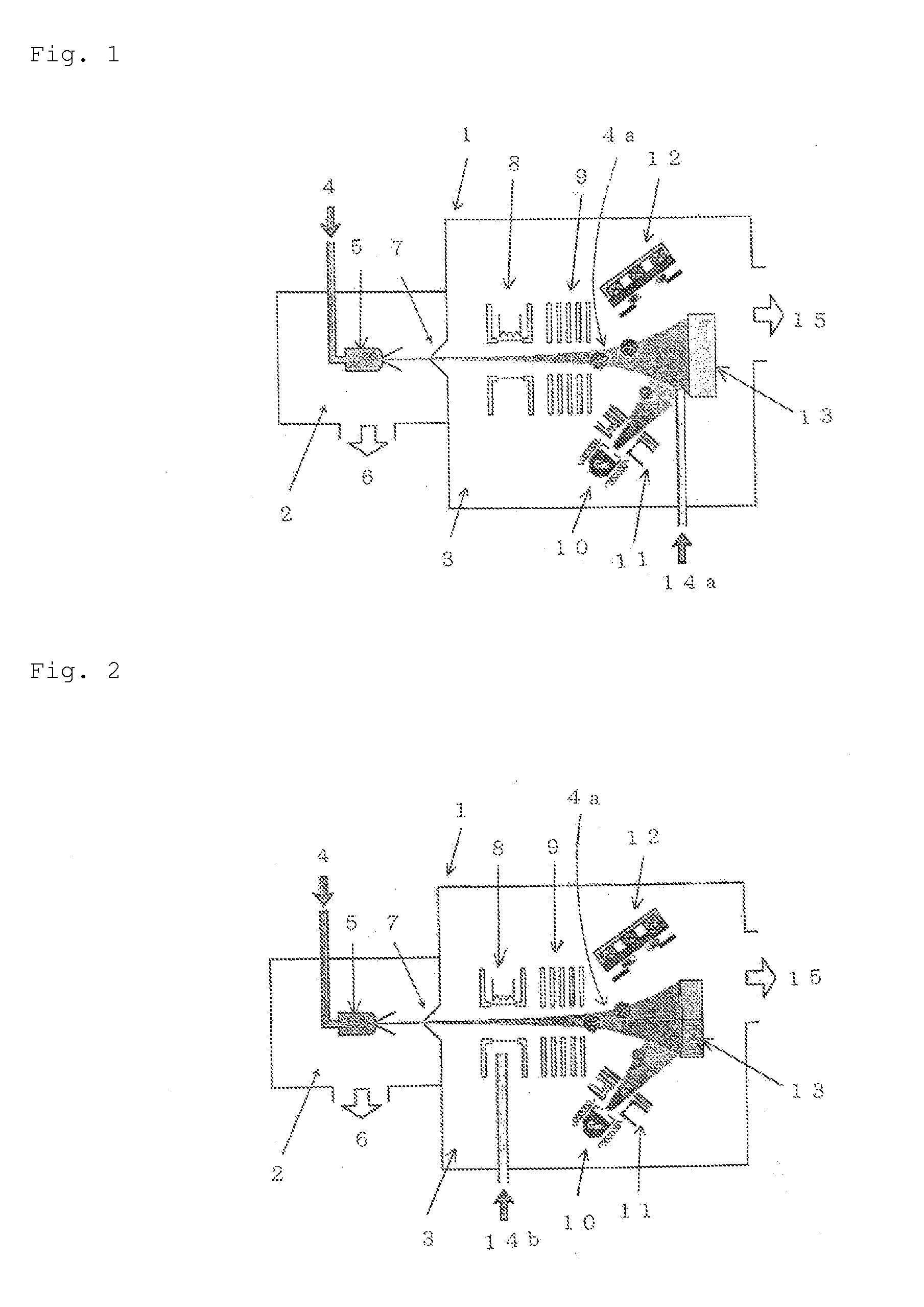
[0089]A sample having a boron-containing carbon film containing substantially no hydrogen was prepared in the same manner as in Example 1 (using evaporated particles of diborane as the evaporated particles of a boron material) except that the apparatus shown in FIG. 2 was used.
example 3
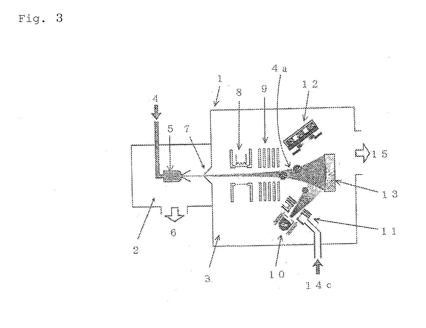
[0090]A sample having a boron-containing carbon film containing substantially no hydrogen was prepared in the same manner as in Example 1 except that trimethoxy boron as the boron material and the apparatus shown in FIG. 2 were used.
PUM
| Property | Measurement | Unit |
|---|---|---|
| volume resistivity | aaaaa | aaaaa |
| thickness | aaaaa | aaaaa |
| temperature | aaaaa | aaaaa |
Abstract
Description
Claims
Application Information