
Method of manufacturing IC comprising a bipolar transistor and IC

a technology of bipolar transistors and manufacturing methods, applied in the direction of transistors, electrical apparatus, semiconductor devices, etc., can solve the problems of limiting the usefulness of cmos transistors in rf applications, prohibiting the use of rf-cmos technologies for manufacturing small volume devices, and increasing the cost of manufacturing integrated circuits based on silicon bipolar transistor technology. , to achieve the effect of reducing base-link resistance and improving cut-off frequency and/or manufactur

Active Publication Date: 2015-02-12
NXP BV
View PDF1 Cites 0 Cited by
  • Summary
  • Abstract
  • Description
  • Claims
  • Application Information

AI Technical Summary

Benefits of technology

This approach reduces base-link resistance while preserving cut-off frequency and manufacturing yield, avoiding adverse effects on doping profiles and emitter sidewall profiles.

Problems solved by technology

However, the manufacture of integrated circuits (ICs) based on silicon bipolar transistor technology is more costly than for instance complementary metal oxide semiconductor (CMOS) ICs, and the downscaling of the device feature size is more easily achieved in CMOS technology.
However, the breakdown characteristics of CMOS transistors limit the usefulness of CMOS transistors in RF applications unless costly measures are implemented in the CMOS process to improve these characteristics.
Such costly measures typically prohibit the use of RF-CMOS technologies for manufacturing small volume devices such as analog mixed signal (AMS) devices.
The challenge that process developers face is that the number of alterations to the CMOS process should remain small whilst at the same time yielding good quality bipolar transistors that are capable of handling high frequency signals.
However, as sidewall spacers 22 are already at a minimal thickness in most process technologies, further lateral size reductions are difficult to achieve such that it appears more promising to attempt to reduce the impact of the etch protection layer portions 20 on the base-link resistance.
A drawback of the known method is that the RF properties of the devices obtained in this matter are unsatisfactory.
These cavities are subsequently filled by a high temperature treatment at 900° C. in a H2 atmosphere, which causes the migration of some of the polysilicon forming the base contact layer into the cavities, thereby substantially filling these cavities, which reduces the base-link resistance.
However, this approach still suffers from some drawbacks.
When using polysilicon as the migratory material, a high temperature of at least 900° C. has to be used to achieve the migration into the cavities, but at such temperatures diffusion of (vertical) doping profiles such as the npn doping profile cannot be avoided, which negatively affects the cut-off frequency fT of the transistor due to the increase in the major carrier delay times caused by the diffusion of these doping profiles.
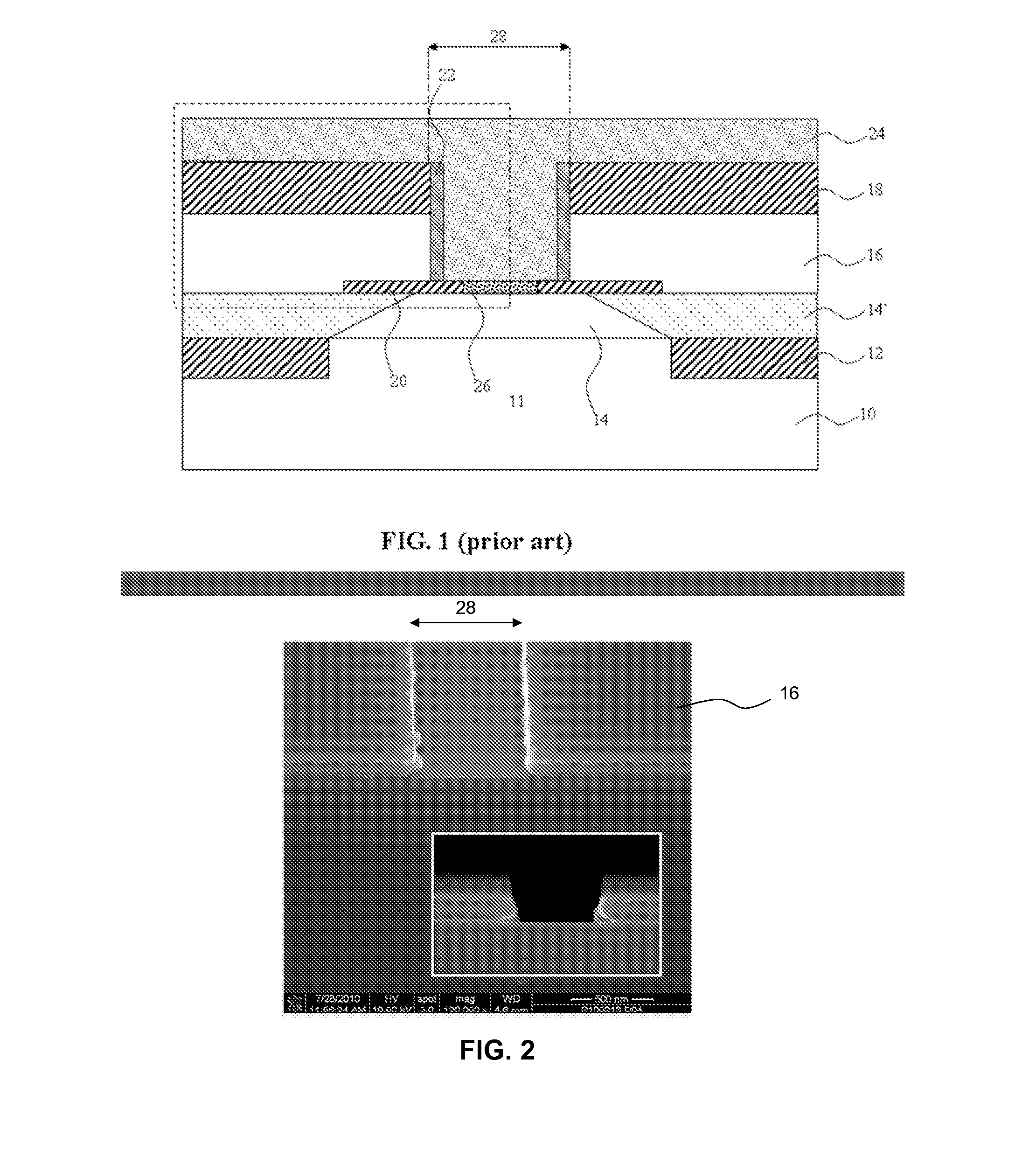
Alternatively, when using SiGe as the migratory material, the migration can be achieved at lower temperatures, i.e. around 800° C., but as demonstrated in FIG. 2, which depicts a bipolar transistor having a SiGe base contact layer 16 subjected to such a thermal treatment, the smoothness of the sidewalls of the emitter window 28 is negatively affected, which complicates the further processing of the bipolar transistor, thus causing both yield and transistor performance issues.

Method used


Image

  • Method of manufacturing IC comprising a bipolar transistor and IC
  • Method of manufacturing IC comprising a bipolar transistor and IC
  • Method of manufacturing IC comprising a bipolar transistor and IC

Examples


Embodiment Construction

[0022]Embodiments of the invention are described in more detail and by way of non-limiting examples with reference to the accompanying drawings, wherein:

[0023]FIG. 1 schematically depicts a prior art bipolar transistor;

[0024]FIG. 2 show a scanning electron microscopic image of a prior art bipolar transistor;

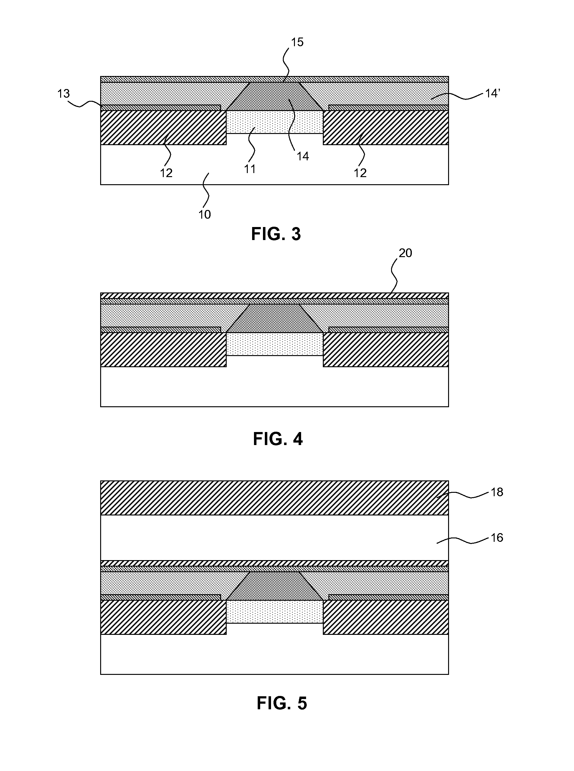
[0025]FIG. 3-8 schematically depict various steps of an IC manufacturing method according to an embodiment of the present invention; and

[0026]FIG. 9 schematically depicts an aspect of an IC manufacturing method according to an alternative embodiment of the present invention.

DETAILED DESCRIPTION OF THE DRAWINGS

[0027]It should be understood that the Figures are merely schematic and are not drawn to scale. It should also be understood that the same reference numerals are used throughout the Figures to indicate the same or similar parts.

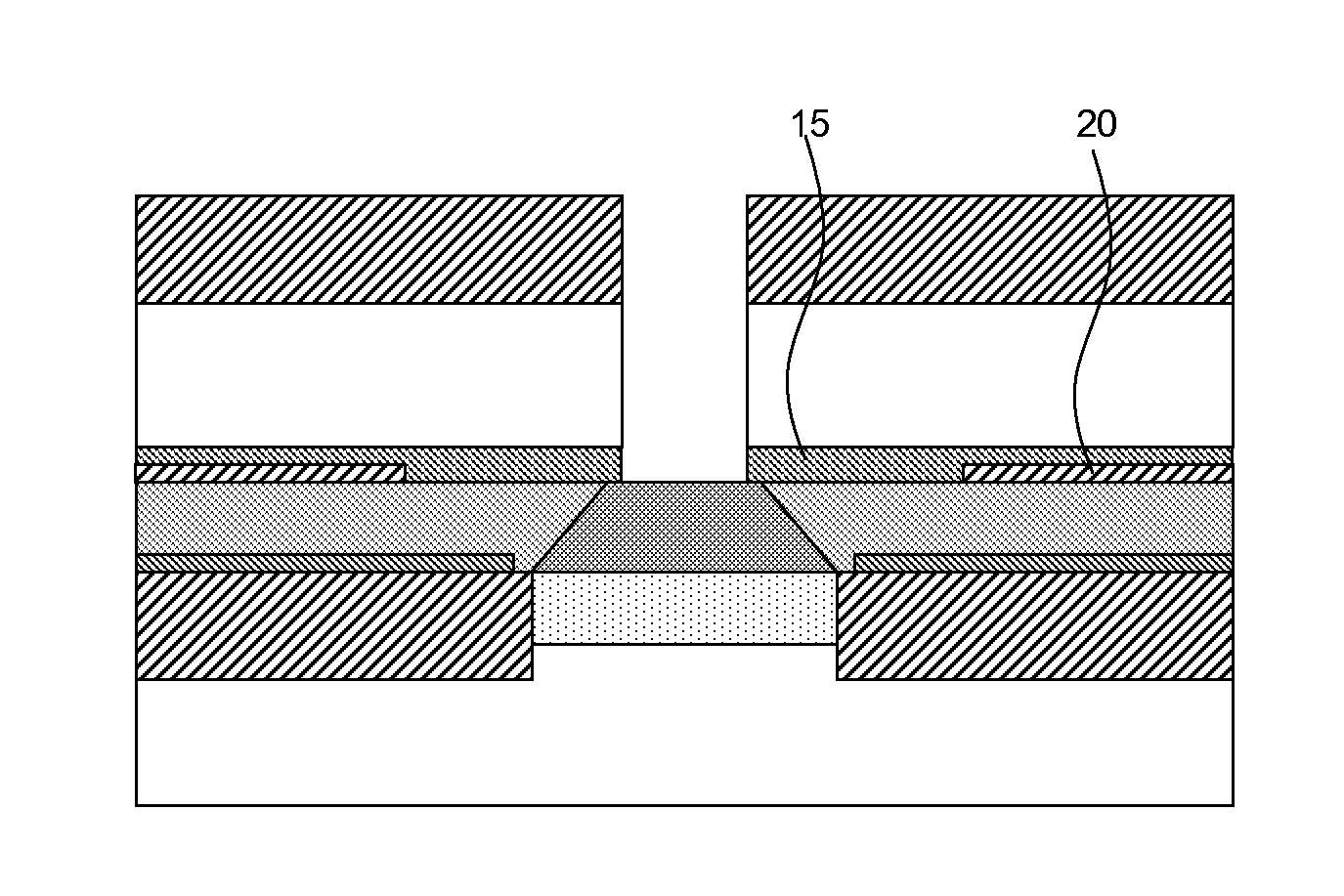
[0028]A possible starting point of the method of the present invention is shown in FIG. 3. A substrate 10 including an active region 11 in between is...


PUM


Abstract

Disclosed is a method of manufacturing an integrated circuit comprising a bipolar transistor, the method comprising providing a substrate (10) comprising a pair of first isolation regions (12) separated from each other by an active region (11) comprising a collector impurity said bipolar transistor; forming a base layer stack (14, 14′) over said substrate; forming a further stack of a migration layer (15) having a first migration temperature and an etch stop layer (20) over said base layer stack (14); forming a base contact layer (16) having a second migration temperature over the further stack, the second migration temperature being higher than the first migration temperature; etching an emitter window (28) in the base contact layer over the active region, said etching step terminating at the etch stop layer; at least partially removing the etch stop layer, thereby forming cavities (29) extending from the emitter window in between the base contact layer and the redistribution layer; and exposing the resultant structure to the first migration temperature in a hydrogen atmosphere, thereby filling the cavities with the migration layer material. An IC comprising such a bipolar transistor is also disclosed.

Description

FIELD OF THE INVENTION[0001]The invention relates to a method of manufacturing an integrated circuit comprising a bipolar transistor.[0002]The present invention further relates to an integrated circuit comprising a bipolar transistor.BACKGROUND OF THE INVENTION[0003]Nowadays, many electronic devices incorporate functionality that operates at radio frequencies, such as mobile communication devices. The implementation of such functionality in a cost-effective manner is far from trivial. It is well-known that bipolar transistors are particularly suitable for handling signals in the radio frequency (RF) domain. However, the manufacture of integrated circuits (ICs) based on silicon bipolar transistor technology is more costly than for instance complementary metal oxide semiconductor (CMOS) ICs, and the downscaling of the device feature size is more easily achieved in CMOS technology. The cost-effective nature of CMOS technology has led to the acceptance of CMOS technology as the mainstre...

Claims


Application Information

Patent Timeline
Patent Type & Authority Applications(United States)
IPC IPC(8): H01L29/737H01L29/45H01L29/10H01L29/161H01L29/165
CPCH01L29/7378H01L29/161H01L29/456H01L29/1004H01L29/165H01L21/8249H01L27/0623H01L29/66242
Inventor DONKERS, JOHANNES JOSEPHUS THEODORUS MARINUSMAGNEE, PETRUS HUBERTUS CORNELISDURIEZ, BLANDINEGRIDELET, EVELYNEMERTENS, HANSVANHOUCKE, TONY
Owner NXP BV
Learn More