Wide bandgap insulated gate semiconductor device

a technology of insulated gate and semiconductor, applied in the direction of semiconductor devices, basic electric elements, electrical equipment, etc., can solve the problems of increasing the electric field across increasing the risk of damage and increasing the risk of excessive electric field applied to the gate insulating film on the trench bottom. , to achieve the effect of reducing the resistance of the drift layer, reducing the spread of the depletion layer, and increasing the concentration of impur

Active Publication Date: 2015-02-26
FUJI ELECTRIC CO LTD
View PDF5 Cites 41 Cited by
  • Summary
  • Abstract
  • Description
  • Claims
  • Application Information

AI Technical Summary

Benefits of technology

[0017]As described above, one of the advantages of wide bandgap semiconductor is that the electric breakdown field is higher than a silicon (Si) semiconductor, thus making it possible to increase the impurity concentration (lower the resistance) of the drift layer even if the breakdown voltage is the same. Furthermore, the spread of the depletion layer being lessened makes it possible for the wide bandgap semiconductor to reduce the required thickness of the drift layer and to further lower resistance.

Problems solved by technology

However, when forming a MOSFET using a wide bandgap semiconductor, the impurity concentration of the drift layer is increased and the thickness thereof is decreased, thereby increasing the electric field of the wide bandgap semiconductor directly below the gate insulating film more than in a Si semiconductor device, and thus causing an increase in the electric field across the gate insulating film; this makes the gate insulating film more susceptible to being damaged.
In particular, in a trench gate MOSFET, there is no pinch-off caused by the JFET effect as in a planar gate structure, and thus the gate insulating film on the trench bottom is more susceptible to having an excessive electric field applied thereto.
However, when the parasitic transistor is pinched off, the on-resistance will increase due to the JFET effect, and thus a trade-off can be seen between reducing the electric field applied to the gate insulting film and lowering the on-resistance.

Method used


Image

  • Wide bandgap insulated gate semiconductor device
  • Wide bandgap insulated gate semiconductor device
  • Wide bandgap insulated gate semiconductor device

Examples


embodiment 1

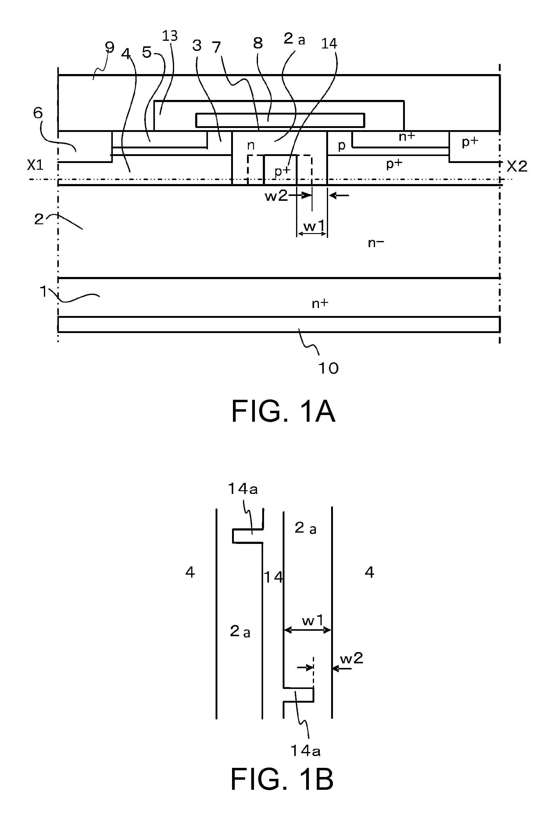
[0044]FIG. 1A is a vertical cross-sectional view (hereinafter, cross-sectional view) of a semiconductor substrate of a single cell of a SiC-MOSFET according to Embodiment 1 of the present invention, and FIG. 1B is a horizontal cross-sectional view of FIG. 1A along the line X1-X2. FIG. 1B shows the a JFET region 2a appearing on the surface of the horizontal cross-sectional view in FIG. 1A as a stripe shape in a plan view. FIG. 1A differs from the cross-sectional view of the conventional cell shown in FIG. 8 in that a floating p+ region 14 is simultaneously formed along with a p+ base region 4 on a portion inside the JFET region 2a. As shown in FIG. 1B, in this embodiment, protruding parts 14a are provided on portions of respective side faces of the floating p+ region 14 that face the respective side faces of the p+ base region 4 in a plan view. In this disclosure, the JFET region 2a may also be referred to as a protruding drift layer portion since it is connected to the drift layer 2...

embodiment 2

[0048]FIG. 4 is a vertical cross-sectional view of a single cell of an SiC-IGBT (insulated gate bipolar transistor) semiconductor substrate according to Embodiment 2 of the present invention. FIG. 4 differs from FIGS. 1A and 1B in that a p-type semiconductor substrate (p+ substrate 11) with a high impurity concentration is provided instead of the n+ substrate 1, and an n-type buffer layer 12 (or a field stop layer) is disposed between an n− drift layer 2 and the p+ substrate 11. Furthermore, in the IGBT, the terms emitter and collector are used instead of source / drain as used for the MOSFET above. As before, in a horizontal cross-sectional view along the line X5-X6 in FIG. 4, the striped surface cell pattern or the hexagonal surface cell pattern can each achieve effects similar to Embodiment 1.

[0049]MOSFETs are unipolar, and fundamentally have no conductivity modulation; thus, MOSFETs are commonly used for devices with low breakdown voltage. As a result, the channel resistance compo...

embodiment 3

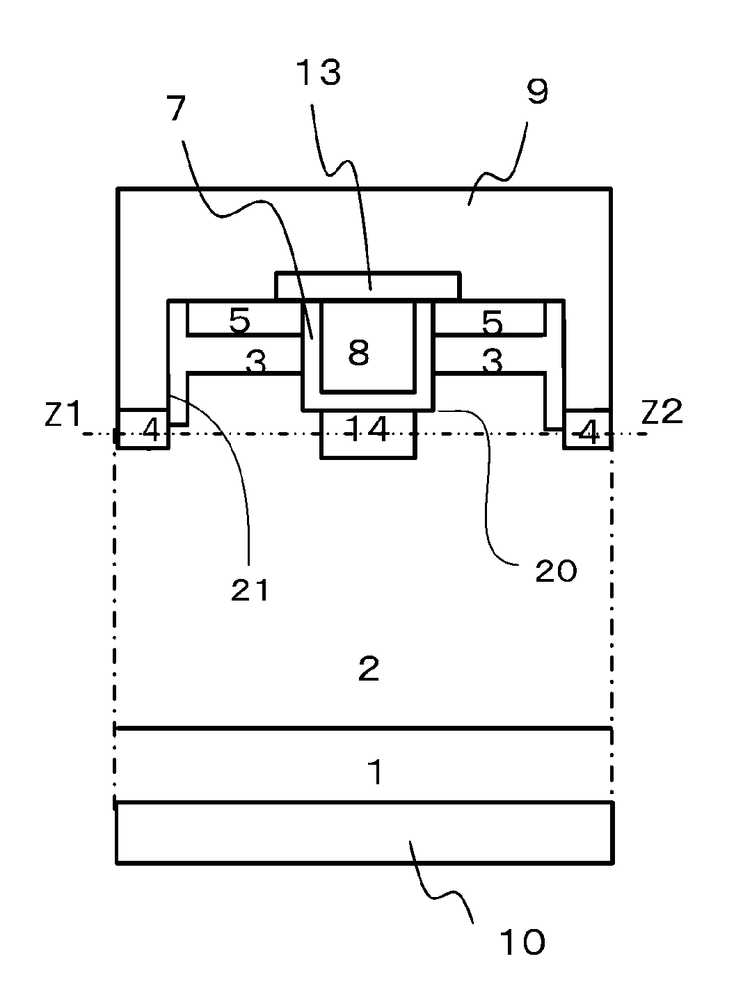
[0051]FIG. 5 is a vertical cross-sectional view of a single cell of a trench gate SiC-MOSFET according to Embodiment 3 of the present invention. In FIG. 5, a floating p+ region 14 is formed below a first trench 20 with a gap therebetween, and the first trench 20 is where a gate electrode 8 is embedded across a gate insulating film 7. A p+ region 4 is formed by an embedded epitaxial method, for example, directly below the bottom of a second trench 21, which is where a source electrode 9 is embedded. In FIG. 5, the floating p+ region 14 is formed in an area directly below the gate insulating film 7 and is separated therefrom as described above to prevent potential adverse effects on a gate insulating film 7. But these may also be in contact with each other in appropriate cases. The plan view shape of the floating p+ region 14 and the p+ base region 4 in a horizontal cross-sectional along the line Y1-Y2 in FIG. 5 may be a striped cell pattern or a hexagonal surface cell pattern, and an...


PUM

PropertyMeasurementUnit
conductivityaaaaaaaaaa
concentrationaaaaaaaaaa
impurity concentrationaaaaaaaaaa

Abstract

A wide bandgap insulated gate semiconductor device includes a semiconductor substrate made of semiconductor having a bandgap wider than silicon; n drift layer over the semiconductor substrate; p-channel regions selectively disposed over the drift layer; n+ semiconductor regions selectively disposed in respective surfaces in the channel regions; a plurality of p+ base regions in contact with bottoms of the respective channel regions; a protruding drift layer portion that is n-type region interposed between the p-channel regions and the p+ base regions thereunder; a gate electrode formed, through a gate insulating film, on the protruding drift layer portion and on respective surfaces of the p-channel regions; a source electrode in contact with the n+ semiconductor regions in the channel regions; and a p+ floating region inside the protruding drift layer portion, having side faces respectively facing side faces of the second conductivity type base regions, wherein respective gaps between the p+ base regions and the p+ floating region defined by the respective side faces have a wide portion and a narrow portion.

Description

BACKGROUND OF THE INVENTION[0001]1. Field of the Invention[0002]The present invention relates to a wide bandgap insulated gate semiconductor device for use with inverters, switching power sources, and the like.[0003]2. Description of Related Art[0004]Due to excellent characteristics such as a high electric breakdown field and high heat transmittance, there is an expectation that wide bandgap semiconductors such as silicon carbide (hereinafter, SiC), gallium nitride (GaN), and diamond will be used for power devices that require a particularly high breakdown voltage and that need to be low loss.[0005]FIG. 8 is a cross-sectional view of a single cell of a conventional planar gate SiC vertical power MOSFET. In FIG. 8, a low impurity concentration n-type drift layer is deposited by SiC epitaxial growth on an n-type SiC semiconductor substrate (n+ substrate 1) with a high impurity concentration. A plurality of p-channel regions 3 are formed on portions of the surface of this low impurity ...

Claims


Application Information

Patent Timeline
Patent Type & Authority Applications(United States)
IPC IPC(8): H01L29/739H01L29/20H01L29/16
CPCH01L29/7395H01L29/2003H01L29/1602H01L29/1608H01L29/41766H01L29/7397H01L29/7802H01L29/7813H01L29/0623H01L29/0878H01L29/1095H01L29/0615H01L29/41741
Inventor KUMAGAI, NAOKI
Owner FUJI ELECTRIC CO LTD
Why Eureka
Try Eureka