Film formation method and film formation apparatus

a film formation and film technology, applied in the direction of vacuum evaporation coating, chemical vapor deposition coating, coating, etc., can solve the problem of difficult to supply a constant amount of pmda into the film formation unit intermittently and stably

Active Publication Date: 2015-03-05
TOKYO ELECTRON LTD +1
View PDF56 Cites 62 Cited by
  • Summary
  • Abstract
  • Description
  • Claims
  • Application Information

AI Technical Summary

Problems solved by technology

However, a problem caused by an acetic acid component remaining in PMDA after this material purification is that it is difficult to supply a constant amount of PMDA into a film formation unit intermittently and stably.
Such an adverse effect caused by an impurity component at a time of supplying a raw material gas is not limited to that at a time of film formation of a polyimide film but is also a problem at a time when another organic film or an organic / inorganic composite film is film-formed.

Method used


Image

  • Film formation method and film formation apparatus
  • Film formation method and film formation apparatus
  • Film formation method and film formation apparatus

Examples


first embodiment

[0096]An embodiment will be described for confirming a problem in a method for removing an impurity in a PMDA raw material according to a conventional method.

[0097]A PMDA raw material with a concentration of acetic acid being 1000 ppm or less and concentrations of aluminum (Al), boron (B), calcium (Ca), cadmium (Cd), cobalt (Co), chromium (Cr), copper (Cu), iron (Fe), potassium (K), lithium (Li), magnesium (Mg), manganese (Mn), sodium (Na), nickel (Ni), lead (Pb), antimony (Sb), titanium (Ti), vanadium (V), and zinc (Zn) being 100 ppb or less was used in all the following embodiments.

[0098]FIG. 6 illustrates a schematic diagram for illustrating a relationship between a PMDA raw material and a concentration of acetic acid. More specifically, FIG. 6 is a schematic diagram of a change in a concentration of an acetic acid in a system (in a gas phase) in a case where an acetic acid and / or acetic anhydride removal treatment was applied to a PMDA raw material for 8.5 hours according to the...

second embodiment

[0100]An embodiment will be described for confirming that it was possible to supply a certain amount of PMDA into a film formation apparatus intermittently by removing an impurity in a PMDA raw material.

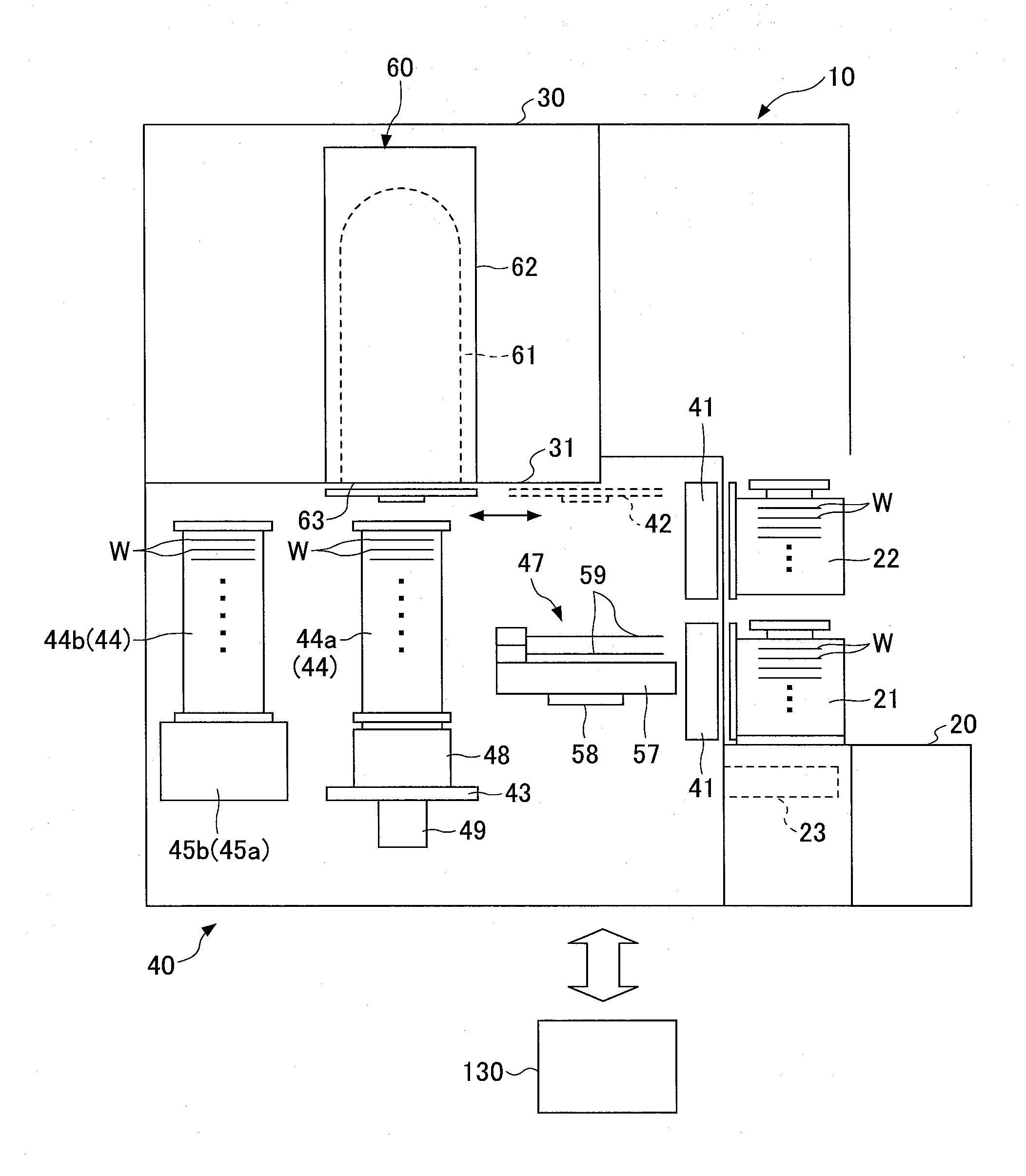
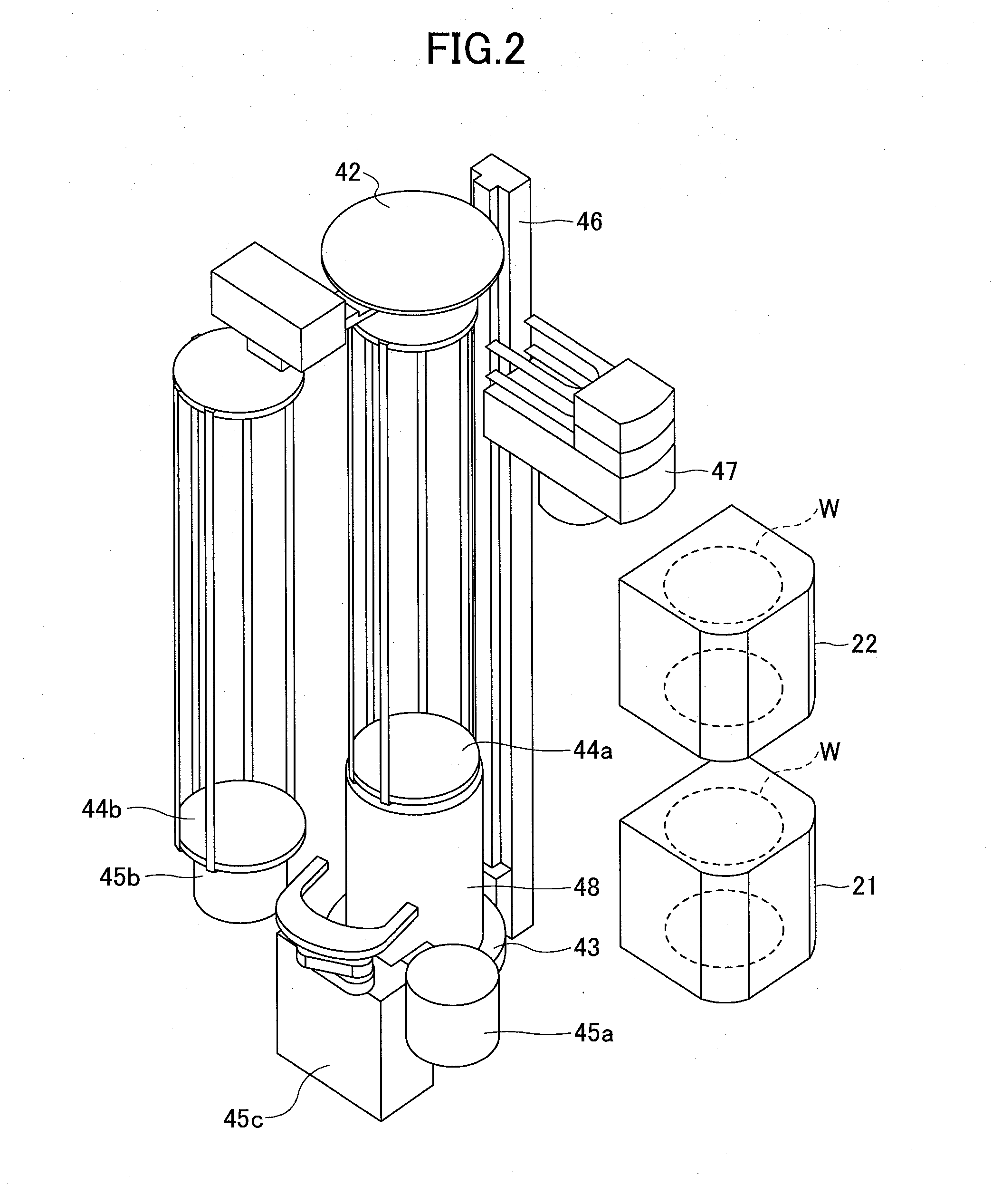
[0101]Here, the film formation unit 60 described with FIG. 4 was used for a film formation unit in all the following embodiments. Furthermore, 8 trays made of stainless steel that were tray 1-tray 8 were arranged at a predetermined interval in order from a bottom in a vertical direction in the PMDA vaporizer 71b and a PMDA raw material was received in each tray. Furthermore, the gasket filter 78 was arranged at a downstream side of the vaporizer 71b.

[0102]First, a PMDA raw material described above was put into the PMDA vaporizer 71b in the film formation unit 60 in FIGS. 4 and 77c was opened and the valve 77b was closed to reduce a pressure of the inside of the PMDA vaporizer 71b on a condition that the valve 81b was opened to providing a carrier gas for purging to the PMDA vaporize...

third embodiment

[0117]An embodiment will be described for confirming a relationship between a flow rate of a carrier gas and the efficiency of removal of an acetic acid and / or acetic anhydride component(s) in a film formation method in the present embodiment.

[0118]FIG. 12 illustrates a schematic diagram for illustrating a relationship between a flow rate of a carrier gas and the efficiency of removal of an acetic acid and / or acetic anhydride component(s) in a film formation method according to the present embodiment. In FIG. 12, a horizontal axis indicates a period of time for removal of an acetic acid and / or acid anhydride component(s) and a vertical axis indicates a concentration of acetic acid in a PMDA raw material.

[0119]As is clear from FIG. 12, it could be found that it was possible to remove an acetic acid and / or acetic anhydride component(s) more efficiently by increasing a flow rate of a carrier gas in a range of a flow rate of a carrier gas in the present embodiment.

[0120]Furthermore, FIG...


PUM

PropertyMeasurementUnit
temperatureaaaaaaaaaa
flow rateaaaaaaaaaa
pressureaaaaaaaaaa

Abstract

Disclosed is a film formation method, including vaporizing a plurality of raw material monomers in respective corresponding vaporizers, supplying the plurality of raw material monomers into a film formation apparatus, causing vapor deposition polymerization of the plurality of raw material monomers in the film formation apparatus to form an organic film on a substrate, and removing an impurity contained in at least one raw material monomer among the plurality of raw material monomers before the vapor deposition polymerization.

Description

BACKGROUND OF THE INVENTION[0001]1. Field of the Invention[0002]An aspect of the present invention relates to at least one of a film formation method and a film formation apparatus.[0003]2. Description of the Related Art[0004]In recent years, a range of materials used for semiconductor devices is transitioning from an inorganic material to an organic material and an organic-inorganic hybrid material. In order to optimize the characteristic of or the manufacturing process for a semiconductor device, a high level of design of a material is being conducted by utilizing a difference between material characteristics of an organic material and an inorganic material.[0005]For one of such organic materials, it is possible to provide a polyimide. A polyimide is excellent as an insulating property thereof, and hence, it is possible to be used for an insulting film in a semiconductor device.[0006]For one example of a method for film-forming a polyimide film, a film formation method based on va...

Claims


Application Information

Patent Timeline
Patent Type & Authority Applications(United States)
IPC IPC(8): H01L21/02C23C14/24C23C14/54C23C14/12
CPCH01L21/02312C23C14/12H01L21/02118C23C14/54H01L21/02271C23C14/24C23C16/44H01L21/02263H01L21/32056H01L21/324H01L21/67017H01L21/67098H01L21/67346
Inventor KUMAGAI, YASUNORITARUTANI, KOHEIKAMEOKA, TAKASHIYANAGITA, TOMOKOMATSUI, RYOHEI
Owner TOKYO ELECTRON LTD
Why Eureka
Try Eureka