

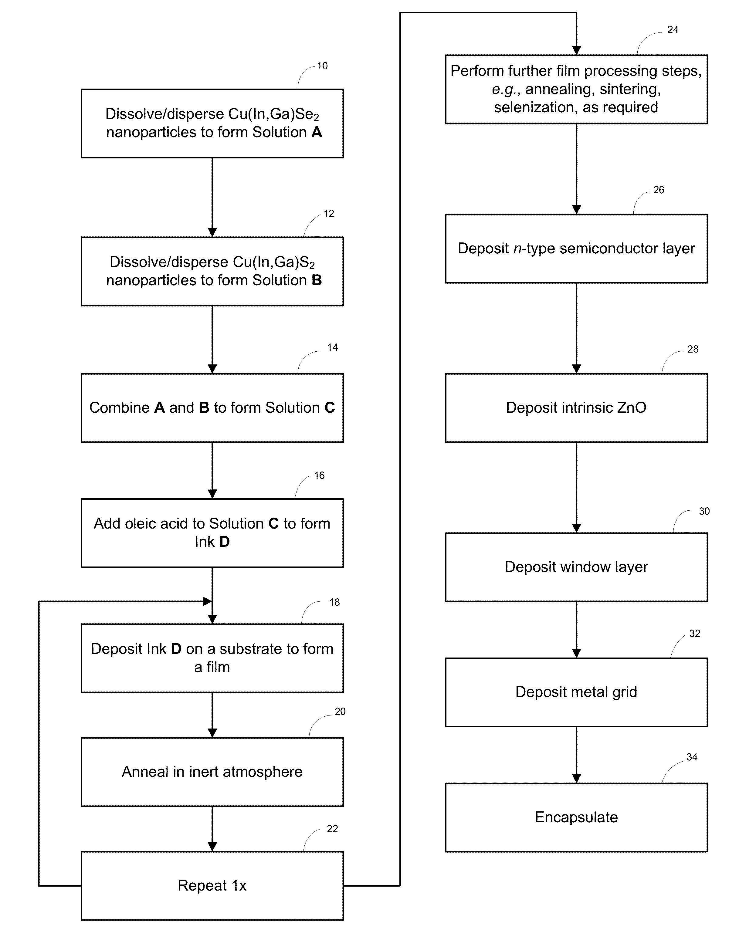
CIGS Nanoparticle Ink Formulation having a High Crack-Free Limit
a nanoparticle and nanoparticle technology, applied in the direction of inks, non-metal conductors, conductors, etc., can solve the problems of high cost of single-crystal wafers, difficult and expensive scaling to larger-area deposition and higher process throughput, and limited control of particle morphology, etc., to achieve the effect of high quality
- Summary
- Abstract
- Description
- Claims
- Application Information
AI Technical Summary
Benefits of technology
Problems solved by technology
Method used
Image

Examples
example 1
GIGS Thin Film Fabricated from a CuInSe2-CuInS2-Oleic Acid (2 wt. %) Ink
[0056]CuInSe2 nanoparticles capped with 1-octane selenol were dissolved in toluene to form a 500 mg / mL solution, E. CuInS2 nanoparticles capped with 1-octane thiol were dissolved in toluene to form a 500 mg / mL solution, F. E and F were combined in a 1:1 ratio to form a solution, G. Oleic acid (2 wt. %) was added to the solution G and shaken to form an ink, H.
[0057]A layer of CuInSe2 was deposited on Mo-coated SLG substrates by spin coating at a concentration of 100 mg / mL, using a spin speed of 2,000 rpm. The layer was annealed at 270° C. for 5 minutes and 415° C. for 5 minutes to remove the ligand, yielding a layer thickness of approximately 50 nm.
[0058]The ink, H, was deposited on top of the CuInSe2 layer by spin coating at a concentration of 500 mg / mL, using a spin speed of 2000 rpm. The film was annealed at 270° C. for 2 minutes, then 415° C. for 2 minutes to remove the organic components of the ink formulati...
example 2
CIGS Thin Film Fabricated from a CuInSe2-CuInS2-Oleic Acid (5 wt. %) Ink
[0061]CuInSe2 nanoparticles capped with 1-octane selenol were dissolved in toluene to form a 500 mg / mL solution, I. CuInS2 nanoparticles capped with 1-octane thiol were dissolved in toluene to form a 500 mg / mL solution, J. I and J were combined in a 1:1 ratio to form a solution, K. Oleic acid (5 wt. %) was added to the solution K and shaken to form an ink, L.
[0062]The ink, L, was deposited on top of Mo-coated SLG by spin coating at a concentration of 500 mg / mL, using a spin speed of 2000 rpm. The film was annealed at 415° C. for 2 minutes to remove the organic components of the ink formulation, forming a 560 nm film. The process was repeated, yielding a total film thickness of 1120 nm.
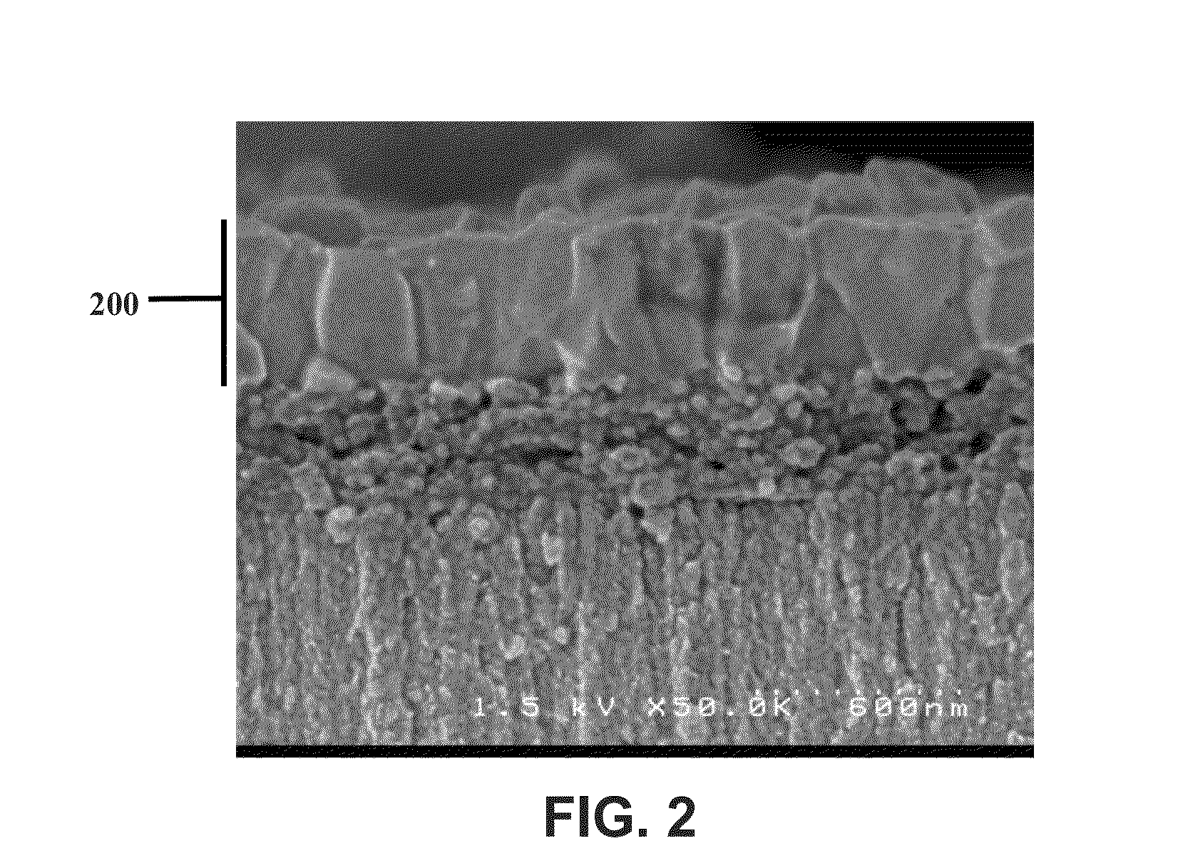
[0063]In optical microscopy images, the film appeared smooth and crack-free after deposition and annealing of the first and second 560 nm CIGS layers, confirming a crack-free limit greater than 500 nm.
PUM
 Abstract
Description
Claims
Application Information