
Method for fabrication of high aspect ratio trenches and formation of nanoscale features therefrom

a high aspect ratio, feature-forming technology, applied in the direction of photomechanical treatment originals, instruments, photomechanical equipment, etc., can solve the problems of increasing the difficulty and cost of precisely controlling and the inability to precisely control the dopant at the nanoscale level. achieve high-aspect ratio nanometer-scale angled features and high-directional mean free paths

Active Publication Date: 2015-04-30
RGT UNIV OF CALIFORNIA
View PDF4 Cites 31 Cited by
  • Summary
  • Abstract
  • Description
  • Claims
  • Application Information

AI Technical Summary

Benefits of technology

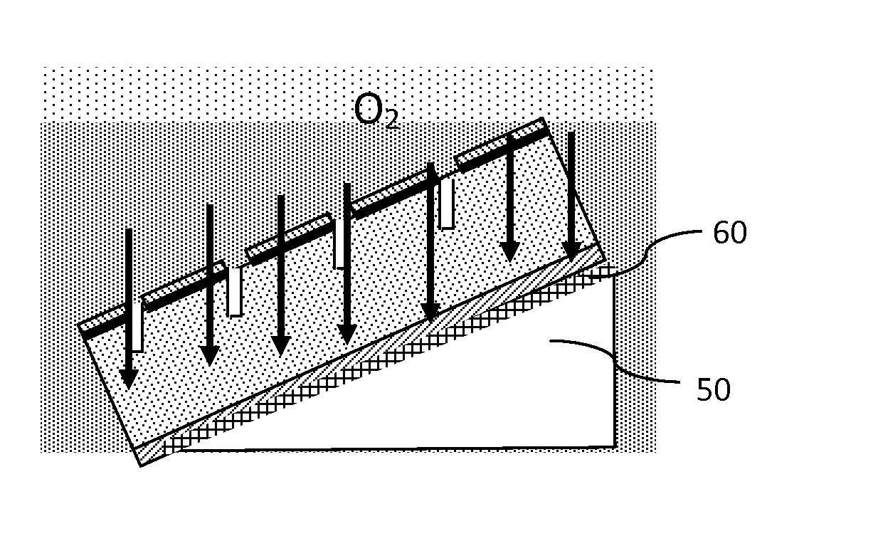
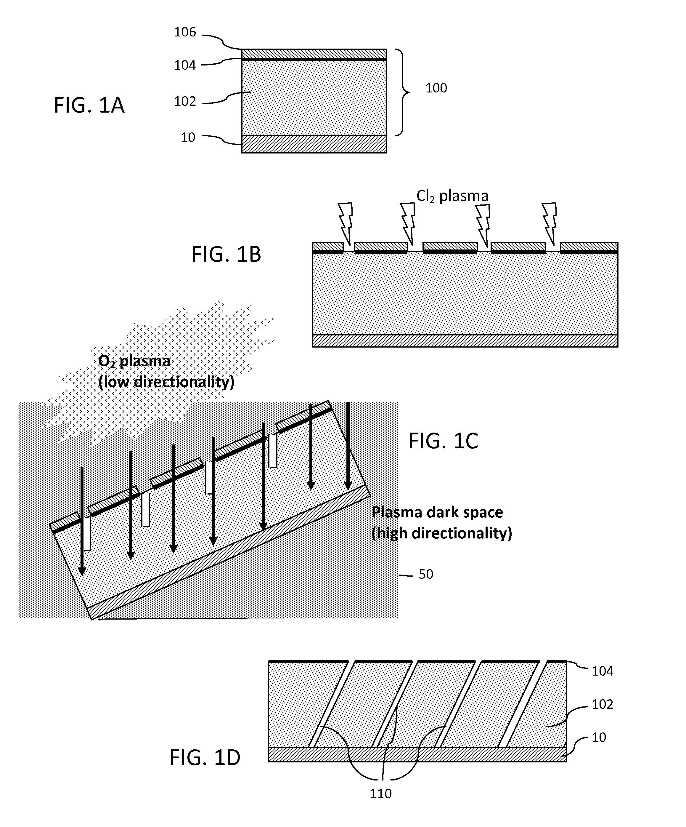
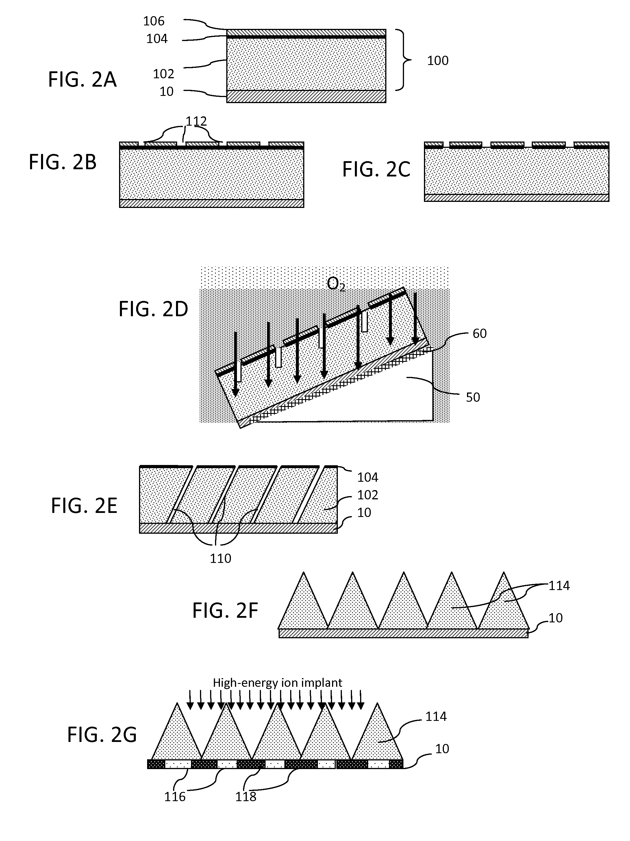
The inventive method described in this patent allows for the fabrication of high-aspect ratio structures in photoresist or device layers using a multilayer approach. The method uses low-pressure RIE to pattern nanometer-scale angled sidewalls and three-dimensional structures in photoresist or directly into a device layer. This approach minimizes undercutting and allows for etching at angles relative to the cathode with high-aspect ratio nanometer-scale angled features. The method can be applied to wafer-scale fabrication and enables production of three-dimensional mask profiles that can be used as masks for ion implantation, as well as formation of MEMS devices, and patterning of materials such as complex oxides used as high-temperature superconductors, SQUID arrays, manganites or other magnetoresistive materials.

Problems solved by technology

As the dimensions of semiconductor devices decrease, it is becoming increasingly difficult and expensive to fabricate nanoscale features and precisely control dopants at the nanoscale level.
For gradient doping, thermal diffusion is typically used to grade the profile which, in practice, is difficult to precisely control at the nanoscale level.
As a result, standard lithography processes are frequently inadequate.
The incident ions accelerated in the plasma are typically directed perpendicular to the sample surface, which, while providing for the formation of features with vertical sidewalls, makes any attempt to perform RIE at a non-perpendicular angle to the surface difficult.
Some publications report efforts to perform angled etching of substrates, however, these approaches typically include complicated sample holders that are limited to either small samples, or fixed angles.
In addition, the described processes may not be used to create high aspect-ratio implant masks.

Method used


Image

  • Method for fabrication of high aspect ratio trenches and formation of nanoscale features therefrom
  • Method for fabrication of high aspect ratio trenches and formation of nanoscale features therefrom
  • Method for fabrication of high aspect ratio trenches and formation of nanoscale features therefrom

Examples


example

Fabrication of SQUID Array

[0050]The inventive process was used for fabricating arrays of nano-superconducting quantum interference devices (SQUIDs) using a high transition temperature (TC) superconducting material such as YBa2Cu3O7-δ (“YBCO”). Substrates consisted of 7×7 mm2 150 nm YBCO files on r-plane sapphire diced from 50.8 mm (2 inch) wafers. The YBCO films are covered by a 15 nm in-situ silver (Ag) film to ensure low contact resistance. In order to allow for robust wire-bonding with good adhesion, an additional 10-nm titanium sticking layer and 200 nm gold layer were sputtered ex-situ. The TC of an unpatterned film has been determined to be approximately 90 K.

[0051]Before patterning of the SQUID array and electrodes, each substrate was stripped of metal at the locations where the SQUID array is to be placed. This step is necessary to ensure that the high-energy ion-radiation used to form the Josephson junctions reaches the YBCO SQUID array without being scattered by the metal ...


PUM

PropertyMeasurementUnit
degree angleaaaaaaaaaa
angleaaaaaaaaaa
thickaaaaaaaaaa

Abstract

A process for forming trenches in a target material includes forming a masking layer onto the target material, where the masking layer comprises a material having high selectivity to a plasma etch gas adapted for etching the target material. A pattern is formed in the masking layer to expose portions of the target material and the sample is placed on an angle mount at a pre-determined angle relative to a cathode of a reactive ion etcher so that the target material is within a plasma dark space of the plasma etch gas. Ballistic ions within the plasma dark space form a trench structure within the target material. The process may further include repeating the steps of positioning the sample and etching the exposed portions of the target material with the substrate at a dif ferent angle to define a triangular structure.

Description

RELATED APPLICATIONS[0001]The present application claims the benefit of the priority of U.S. Provisional Application No. 61 / 651,898, filed May 25, 2012, which is incorporated herein by reference in its entirety.FIELD OF THE INVENTION[0002]The present invention relates to a method for creating masks allowing for high aspect ratio nanometer-scale features and doping profiles.BACKGROUND OF THE INVENTION[0003]As the dimensions of semiconductor devices decrease, it is becoming increasingly difficult and expensive to fabricate nanoscale features and precisely control dopants at the nanoscale level. A great deal of research has been devoted to extending the capabilities of UV lithograph due to its high throughput for manufacturing as compared to direct-write processes such as electron beam lithography. Modern UV lithography machines are rapidly approaching the limits of the smallest features possible, and alternative methods are required to achieve reproducible nanoscale features and dopin...

Claims


Application Information

Patent Timeline
Patent Type & Authority Applications(United States)
IPC IPC(8): H01L21/3065G03F1/80H01L21/311
CPCH01L21/3065G03F1/80H01L21/31116G03F7/094H01L21/31138G01R33/0052B81C1/00103B81B2203/033B81C2201/0132H01J37/34H01L21/302H01L21/308H01J37/20H01J37/3056B81C1/00031
Inventor DYNES, ROBERT C.ROEDIGER, PETERWONG, TRAVISCYBART, SHANE A.
Owner RGT UNIV OF CALIFORNIA
Learn More