
Communication module

a communication module and module technology, applied in the field of communication modules, can solve the problems of signal routing, signal quality degradation, increased mounting steps, etc., and achieve the effects of high shielding characteristics, increased heat dissipation efficiency, and high mounting density

Active Publication Date: 2015-04-30
TAIYO YUDEN KK
View PDF5 Cites 29 Cited by
  • Summary
  • Abstract
  • Description
  • Claims
  • Application Information

AI Technical Summary

Benefits of technology

The present invention aims to provide a mobile phone communication module that is highly functional, compact, and resistant to warping and deformation. The communication module has high heat dissipation efficiency and prevents degradation of high-frequency circuits when multiple parts are mounted together. It is easy to compact and has excellent mounting characteristics.

Problems solved by technology

There were also issues due to the increased number of mounting steps.
Furthermore, since the respective modules are connected through wiring lines on substrates of the respective motherboards and modules, the routing of signals increases and degradation of signal quality occurs.
It is also difficult to decrease the size of the modules as a whole if the modules are each provided with a shield.
Meanwhile, based on the problems concerning conventional mobile phones as described above, there is demand for almost all functions, such as front end components, high frequency IC, power circuit, baseband signal processing circuits, memory, and the like to be provided on a single circuit substrate.
However, if the high-frequency circuit module disclosed in Patent Document 1 has the baseband processing circuit, memory, and power circuit mounted thereon, and the total size is reduced, the following problems would occur: (a) characteristic degradation caused by noise mixing between the respective function parts due to the respective function parts being close to each other, (b) a reduction of heat dissipation efficiency due to the respective function parts being close to each other, and (c) susceptibility to warping during mounting due to the circuit substrate being larger than the preceding high-frequency circuit module, even though the size has been reduced.
Thus, the switching noise generated by the power circuits of the other circuits will electromagnetically couple with the power circuit that supplies power to the high-frequency circuit, resulting in possible degradation of high-frequency characteristics due to the switching noise being transmitted to the high-frequency circuit.
It is also possible that the switching noise generated by the power circuit could cause degradation of the high-frequency characteristics by directly electromagnetically coupling with the high-frequency circuit.

Method used


Image

  • Communication module
  • Communication module
  • Communication module

Examples


embodiment 1

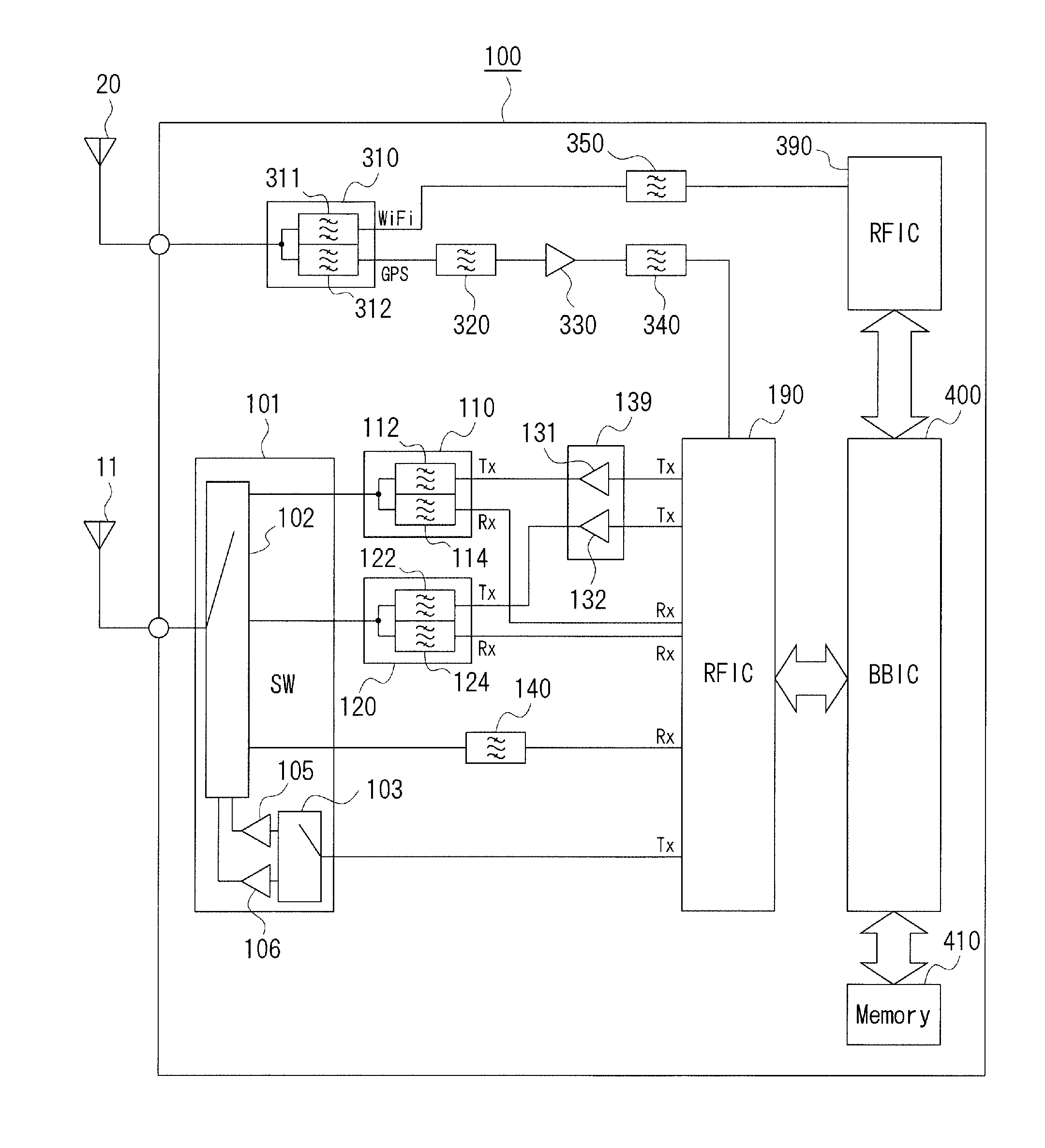
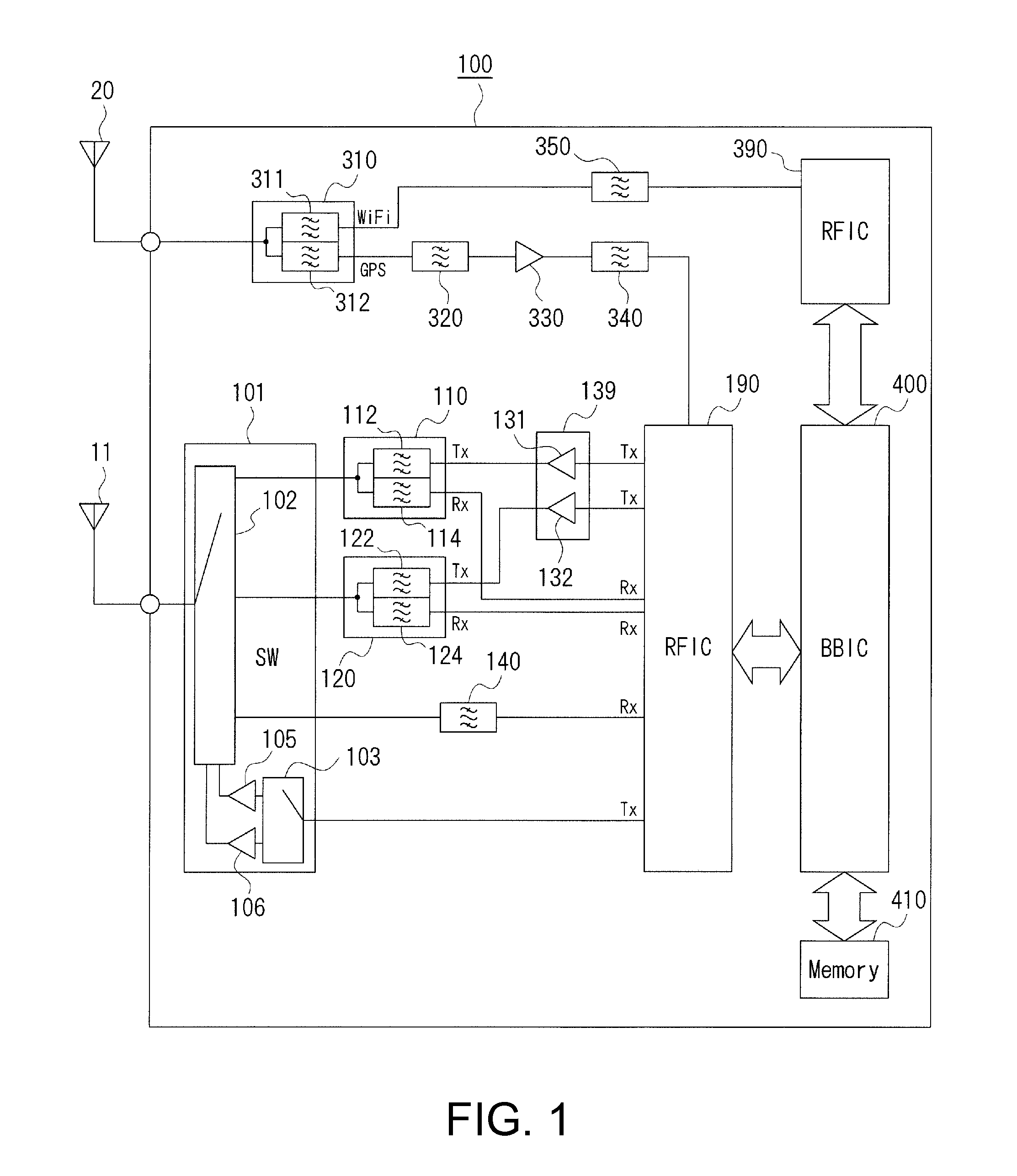
[0034]A communication module according to Embodiment 1 of the present invention will be explained with reference to figures. FIG. 1 is a schematic block view of the communication module. In the present embodiment, for ease of explanation, main configurations relating to the gist of the present invention will be explained.

[0035]A communication module 100 of the present embodiment has the primary functions of the multi-functional mobile phone, the smartphone, integrated into a single module. Specifically, the communication module 100 is provided with various functions such as speech communication on the mobile phone network, which is a broadband wireless communication network, WiFi (registered trademark), which is a form of short-range wireless communication, Bluetooth (registered trademark), and GPS, which is a satellite positioning system. For ease of explanation, the communication module 100 of the present embodiment is assumed to operate in the two W-CDMA (Wideband Code Division M...

embodiment 2

[0068]A communication module according to Embodiment 2 of the present invention will be explained with reference to figures. FIG. 5 is a schematic block view of the communication module. In the present embodiment, for ease of explanation, main configurations relating to the gist of the present invention will be explained. In the present embodiment, elements that are similar to those in Embodiment 1 are given the same reference characters, and an explanation thereof will be omitted.

[0069]As shown in FIG. 5, one point in which a communication module 100′ of the present embodiment differs from the communication module 100 in Embodiment 1 is that the diplexer 310 is omitted due to having a separate GPS antenna 21 and WiFi communication antenna 22 instead. The other circuit configurations are similar to Embodiment 1, and thus, an explanation thereof will be omitted.

[0070]One point in which the communication module 100′ of the present embodiment differs from the communication module 100 i...


PUM


Abstract

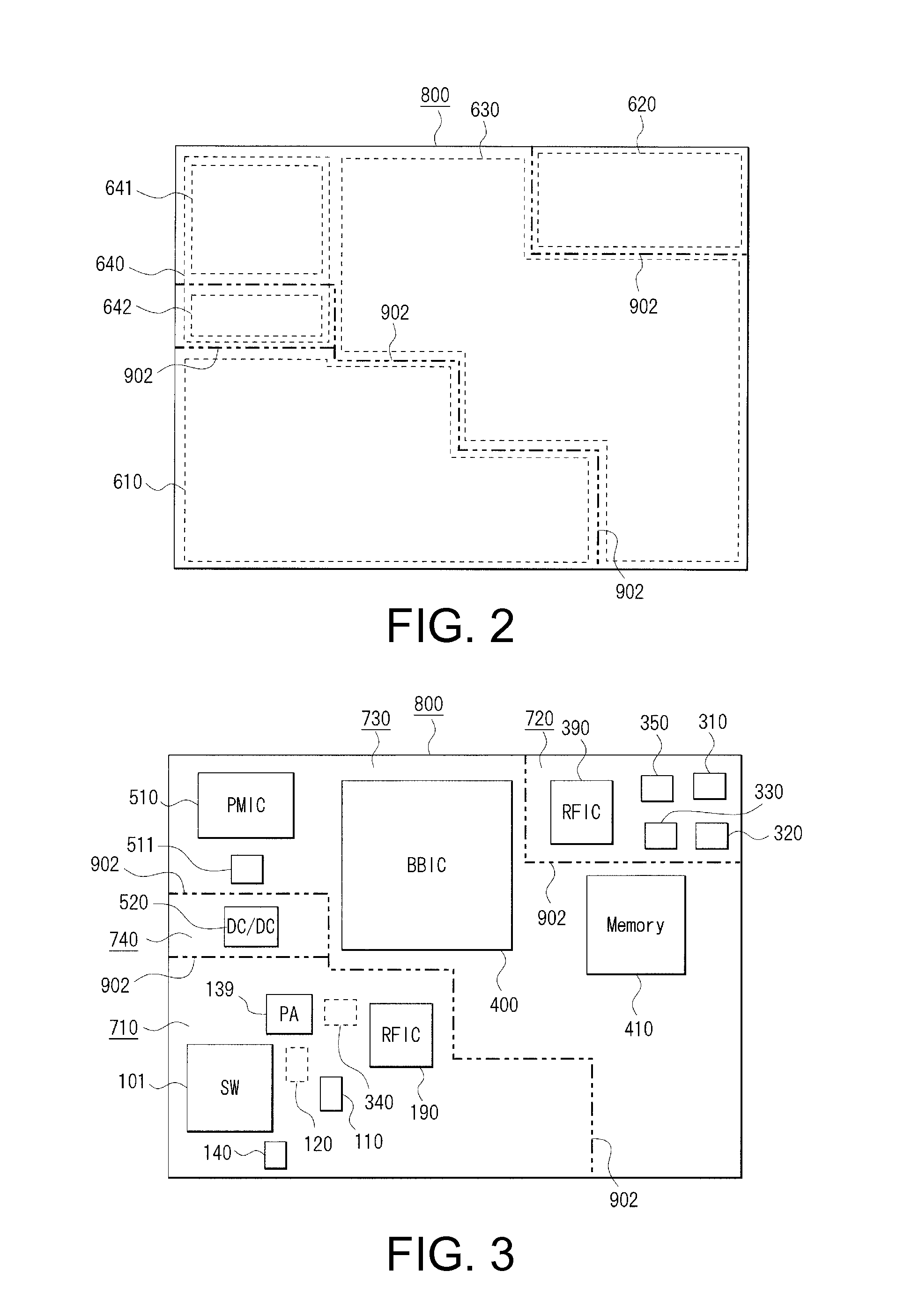
A communication module includes a circuit substrate having a first high-frequency processing section related to mobile phone communication, a second high-frequency processing section that processes reception signals related to satellite positioning systems, a system section having a baseband processing section and application processing section, and a power circuit section, a sealing member covering the electronic components mounted on the circuit substrate, a conductive shield layer formed on a surface of the sealing member, and a shield wall formed in the sealing member so as to demarcate a mounting area of the first high-frequency processing section and a mounting area of the second high-frequency processing section.

Description

BACKGROUND OF THE INVENTION[0001]1. Field of the Invention[0002]The present invention relates to a communication module used in mobile phones.[0003]2. Description of Related Art[0004]Recently, as shown by multi-functional mobile phones such as the smartphone, the functions of mobile phones are increasing and their size is decreasing. Known examples of such a mobile phone include a mobile phone in which a high-frequency circuit module that has various types of front end components necessary for transmission and reception of high-frequency signals mounted together on a circuit substrate is mounted on a motherboard (see Patent Document 1, for example). The term “front end components” means active or passive components for high-frequency signal processing that are arranged on a route between the high-frequency IC, which processes high-frequency signals, and the antenna. In a high-frequency circuit module disclosed in Patent Document 1, front end components such as a power amplifier IC, ...

Claims


Application Information

Patent Timeline
Patent Type & Authority Applications(United States)
IPC IPC(8): H04M1/02
CPCH04M1/026H04B1/38H04B1/3888H04B15/04H05K1/0218H05K3/284H01L2924/0002H05K2201/0715H05K2201/10371H04B15/02H01L2224/16225H05K1/0243H05K9/0022H05K9/0045H01L24/20H01L2224/04105H01L2224/12105H01L2224/73267H01L2924/19105H01L2924/181H01L23/5389H01L24/13H01L24/16H01L23/5384H01L23/5383H01L23/552H01L25/16H01L2225/06517H01L2225/06572H01L2224/131H01L2924/014H01L23/31H01L2924/00
Inventor SAJI, TETSUOICHIKAWA, YOHEINAKAMURA, HIROSHI
Owner TAIYO YUDEN KK
Learn More