Method of treating a surface layer of a device consisting of alumina and respective device, particularly x-ray tube component

a surface layer and alumina technology, applied in the direction of lighting and heating apparatus, charge manipulation, furnaces, etc., can solve the problems of insufficient properties of the deposited layer, deflection of electron beam and electrical breakdown, and similar problems of isolators, etc., to achieve the effect of reducing the resistivity gradient and being easy to adop

Inactive Publication Date: 2015-05-21
KONINKLJIJKE PHILIPS NV
View PDF1 Cites 8 Cited by
  • Summary
  • Abstract
  • Description
  • Claims
  • Application Information

AI Technical Summary

Benefits of technology

[0024]Advantageously, an electrical sheet resistivity gradually increases in the superficial layer region from a lower value at an exposed surface of the surface layer towards an inner portion of the surface layer. In other words, as a result of the treatment method, a decreasing gradient in resistivity between the original alumina in the bulk and more and more of the lower-resistivity material at the surface of the device as a result of the treatment method may occur. This may relax stress due to differences in thermal expansion between the different regions and the materials comprised therein.
[0025]The proposed treatment method may be advantageously applied particularly to miniature components of an electron beam device such as an x-ray tube or an electron gun at least partly enclosing and / or at least partly facing an electron beam in the x-ray tube. Particularly, the method can be easily adopted to processing of large batches or to small parts. Especially for small tubes, the gas of the oxygen-depleted atmosphere may be conducted through the tube or filled into it only, if generation of a low resistivity superficial layer is wanted only on the inner surface of the tube.
[0026]It shall be noted that possible features and advantages of embodiments of the present invention are described herein partly with respect to the proposed treatment method and partly with respect to the proposed device. A person skilled in the art will realize that the described features may be combined or replaced by each other and may be transferred from the method to the device, and vice versa, in order to result in additional embodiments and possibly achieving synergy effects.

Problems solved by technology

In an x-ray tube, electron beams close to insulator parts may result in problems as stray electrons hitting the insulator part may cause charge build-up which can be detrimental to the electrical field and may cause deflection of the electron beam and electrical breakdown.
Similar problems often arise with isolators close to tube anodes (targets), because of scattered electrons and / or secondary electrons from the anode impinging on isolator parts.
However, coating a surface of an isolator part may be time consuming and work intensive, may need specific expensive deposition devices, may require additional handling efforts during device fabrication and, in a worst case, may result in insufficient properties of the deposited layer.
For example, in wet-deposited coatings, problems may occur due to pinholes or uneven deposition.
The quality of coatings may be crucial for grading of a high voltage inside x-ray tubes and e.g. pinholes or thickness gradients may be disastrous.
Furthermore, isolator parts for x-ray tubes may have to be heat-treated at approximately 1000° C. to be vacuum-compatible, which may put high restrictions on matching of thermal expansion of a coating and a substrate material.
Furthermore, particularly in miniature x-ray tubes and miniature electron beam devices, wet-deposition as well as CVD may be difficult and time-consuming because of the small dimensions of such miniature x-ray tubes, of which a tube inner diameter may be e.g. smaller than 2 mm.
Accordingly, for example batch processing may not be straightforward.

Method used


Image

  • Method of treating a surface layer of a device consisting of alumina and respective device, particularly x-ray tube component
  • Method of treating a surface layer of a device consisting of alumina and respective device, particularly x-ray tube component
  • Method of treating a surface layer of a device consisting of alumina and respective device, particularly x-ray tube component

Examples


Embodiment Construction

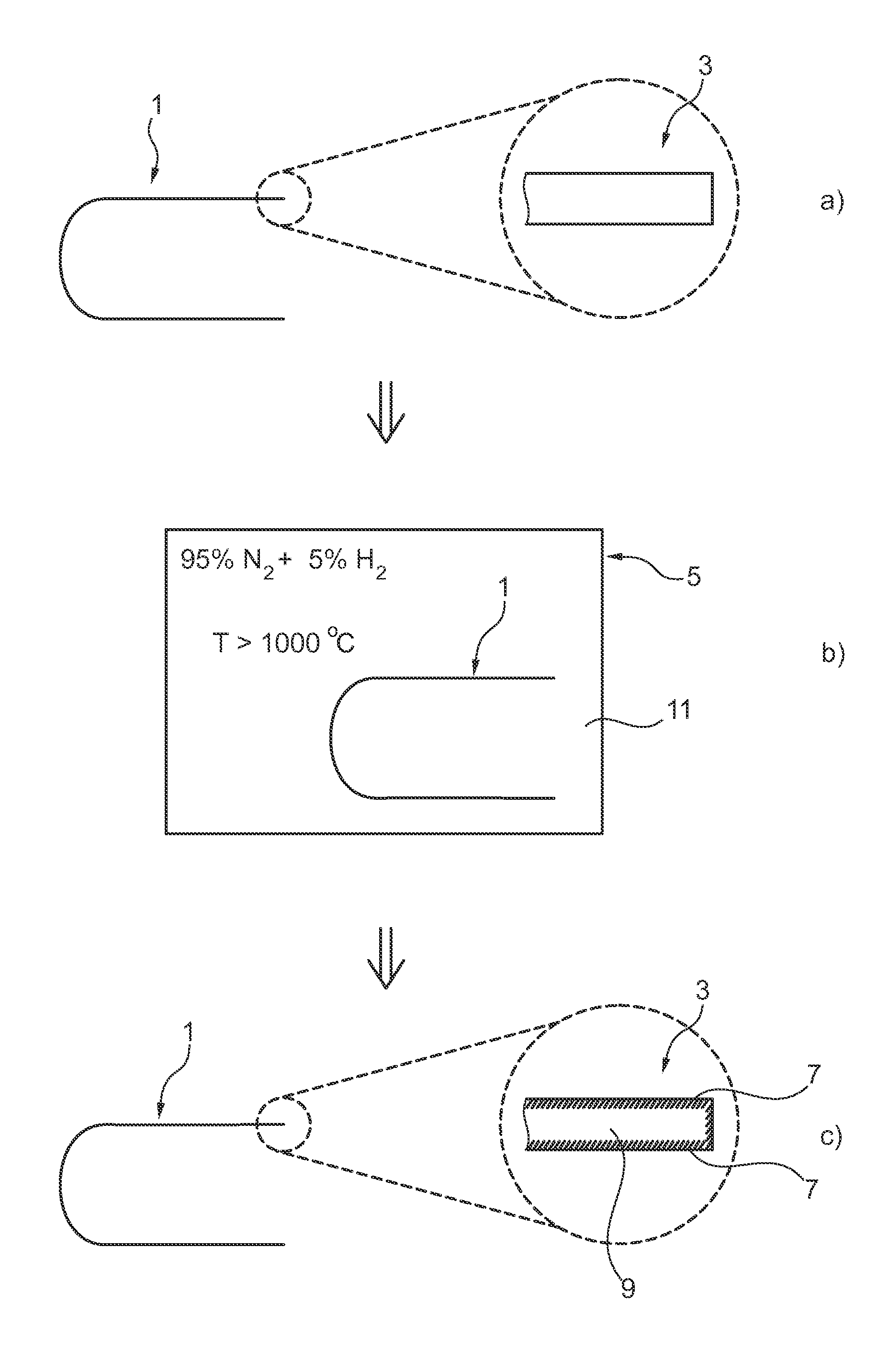
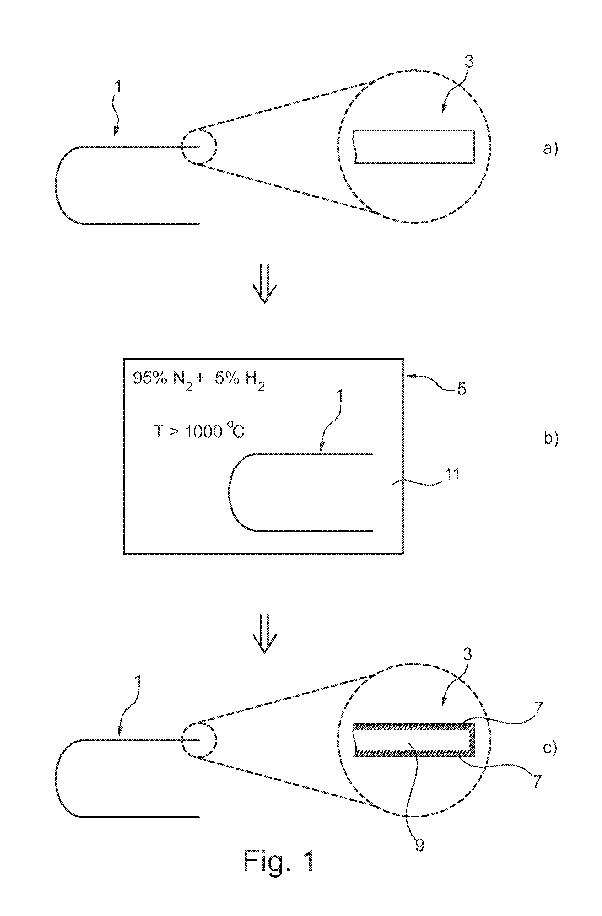
[0030]The method for treating a surface layer of a device consisting of alumina and the resulting device in accordance with an embodiment of the present invention shall be described with reference to FIG. 1.

[0031]A device 1 may have any suitable shape such as a tube, a cylinder, a slab, a bowl, etc and is provided with the surface layer 3 being exposed (FIG. 1(a)). The entire device or at least the surface layer 3 consists of alumina. The device is a component of an x-ray tube or an electron beam device which, at least partly faces an electron beam.

[0032]The device 1 is then placed into an oven 5 (FIG. 1(b)). The oven 5 is filled with an oxygen-depleted atmosphere 11 comprising 95% of nitrogen and 5% at hydrogen. Alternatively, the oven 5 may be filled with argon. The oxygen-depleted atmosphere 11 is heated to an elevated temperature of more than 1700° C. and the device 1 is kept within the oven 5 at this elevated temperature for more than 2 hours.

[0033]After such treatment (FIG. 1(...


PUM

PropertyMeasurementUnit
temperatureaaaaaaaaaa
pressureaaaaaaaaaa

Abstract

A method for treating a surface layer (3) of a device (1) consisting of alumina and a corresponding device (1) are proposed. The method comprises providing the device (1) with the surface layer (3) to be treated being exposed and heating the surface layer (3) of the device (1) in an oxygen-depleted atmosphere comprising e.g. one of an inert gas, nitrogen, hydrogen, argon and a combination thereof to a temperature higher than 1000° C., preferably higher than 1700° C. for a duration of preferably more than 2 hours. Due to such treatment, a superficial layer region (7) comprised in the surface layer (3) may obtain a significantly reduced electrical resistivity which is assumed to be the result of chemically reducing this superficial layer region (7). Such reduced superficial electrical resistivity may advantageously serve for example in components of electron beam devices such as x-ray tube components for preventing any charge build-up.

Description

FIELD OF THE INVENTION[0001]The present invention relates to a method of treating a surface layer of a device which consists of alumina. The invention also relates to a device comprising such conditioned surface layer consisting of alumina. In a specific embodiment, the invention relates to a component of an x-ray tube comprising an alumina surface layer.BACKGROUND OF THE INVENTION[0002]There are many technical devices which completely consist of alumina (e.g. polycrystalline Al2O3) or at least comprise a surface layer consisting of alumina. Alumina, also referred to as aluminium oxide, is frequently used for such devices or for their surface layers due to the superior characteristics of alumina such as high electrical resistivity, high hardness, high resistance to corrosion and weathering, low density, high thermal conductivity, high melting point and excellent vacuum properties. Particularly, as alumina normally is a very good electrical insulator having an electrical bulk resisti...

Claims


Application Information

Patent Timeline
Patent Type & Authority Applications(United States)
IPC IPC(8): C04B41/00H01J35/16
CPCC04B41/0072C04B41/009H01J35/16C04B41/80C04B2111/94C04B35/10C04B41/4517C04B41/455
Inventor RIBBING, CAROLINAMARTINY, CHRISTOPH
Owner KONINKLJIJKE PHILIPS NV
Why Eureka
Try Eureka