finFET isolation by selective cyclic etch

a selective cyclic etch and finfet technology, applied in the direction of semiconductor devices, transistors, electrical apparatus, etc., can solve the problems of inability to control the charge carrier population at increasing, the scaling of traditional designs of devices such as field-effect transistors can compromise electrical characteristics, and the gate voltage is reduced. to achieve the effect of increasing selectivity

Inactive Publication Date: 2015-05-28
GLOBALFOUNDRIES INC
View PDF19 Cites 33 Cited by
  • Summary
  • Abstract
  • Description
  • Claims
  • Application Information

AI Technical Summary

Benefits of technology

[0007]It is therefore an object of the present invention to provide an etching process for semiconductor material and semiconductor oxide of increas

Problems solved by technology

However, scaling of traditional designs of devices such as field-effect transistors can compromise electrical characteristics such as control of the depletion layer in the transistor channel reducing the ratio of resistance in conductive and non-conductive states.
The principal reason for compromise of depletion layer control is that reduced gate voltages necessary to reduce power dissipation requirements are unable to control the charge carrier population at increasing distance from the gate electrode and at corners of the conduction channel, even when the gate insul

Method used


Image

  • finFET isolation by selective cyclic etch
  • finFET isolation by selective cyclic etch
  • finFET isolation by selective cyclic etch

Examples


Embodiment Construction

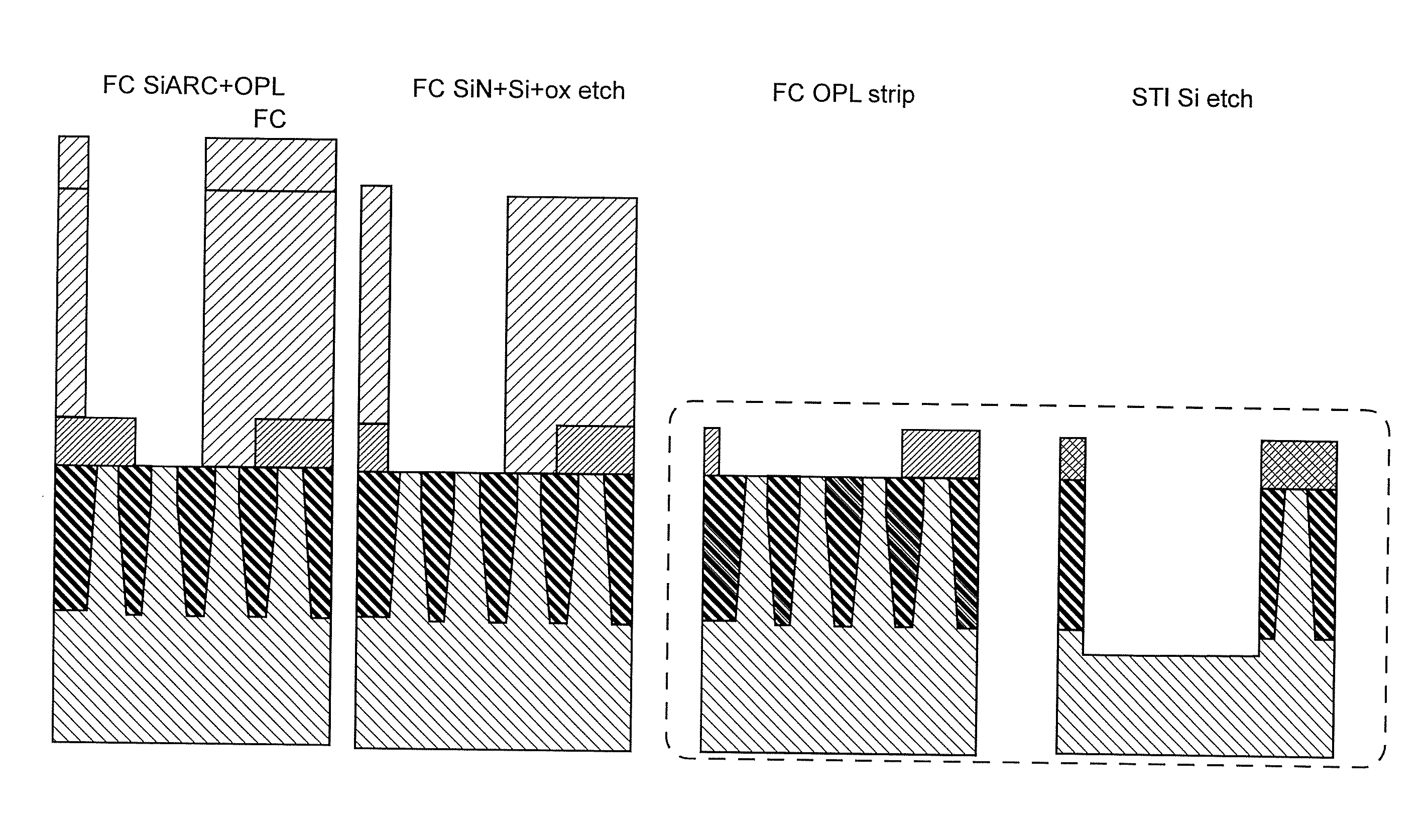
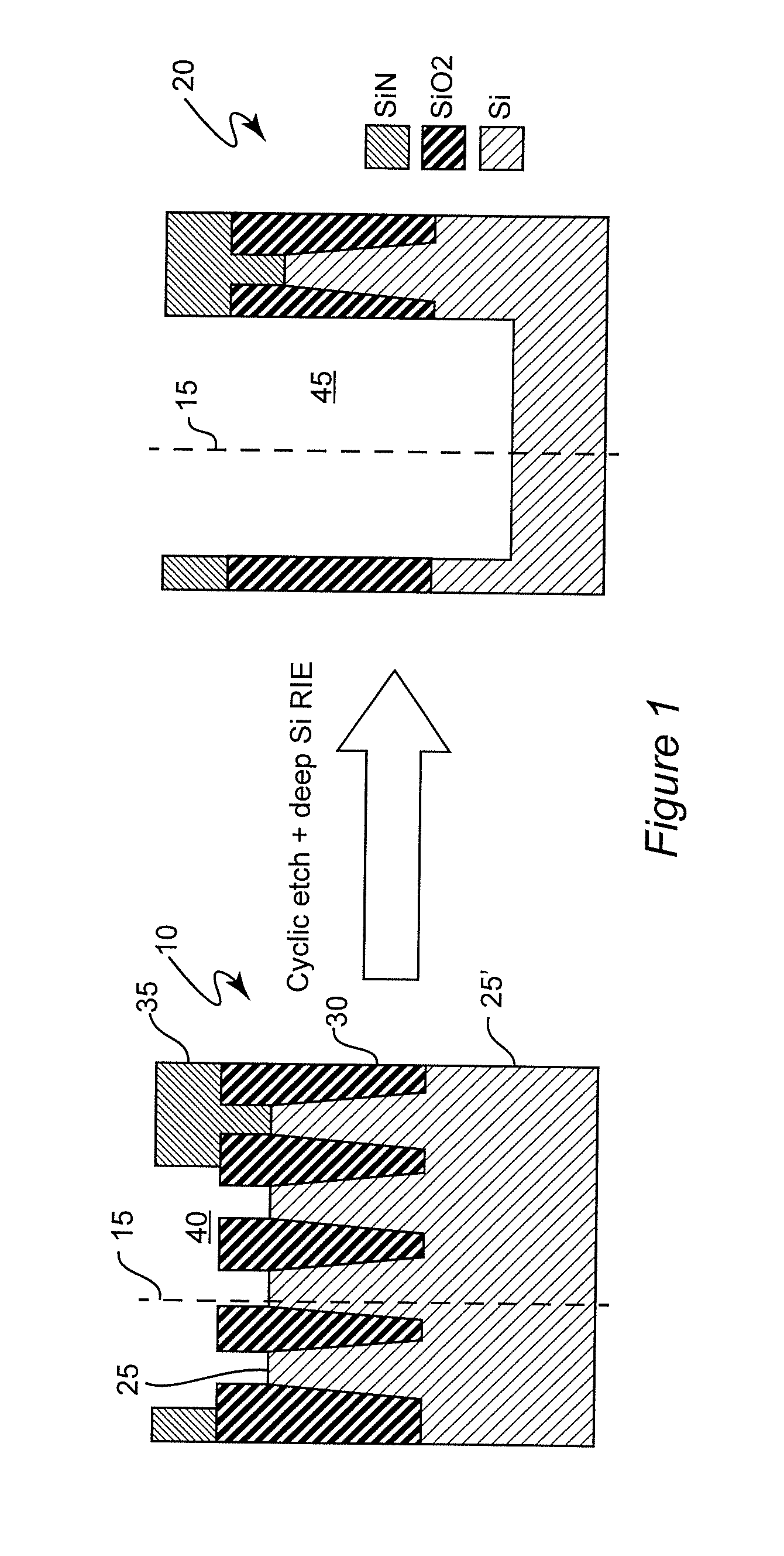
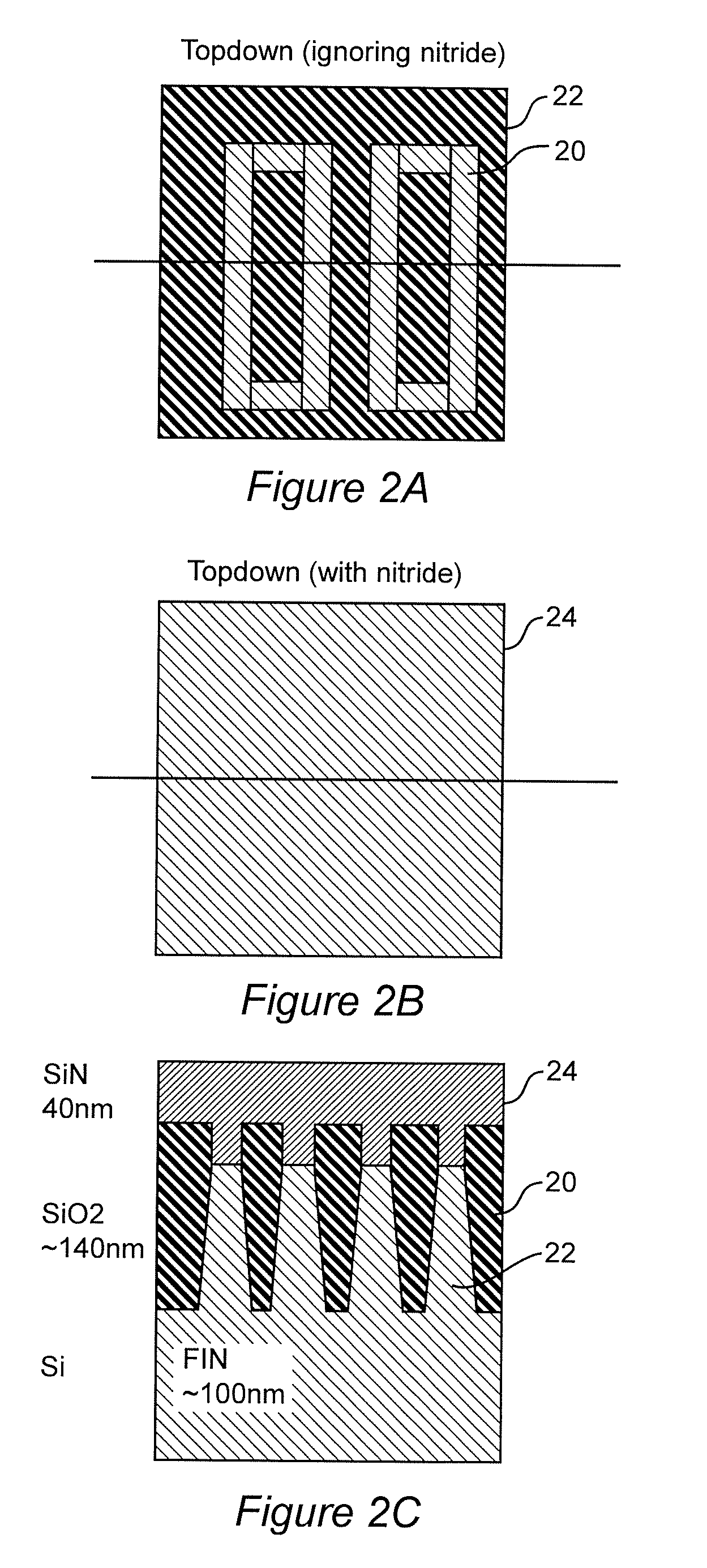
[0021]Referring now to the drawings, and more particularly to FIG. 1, two cross-sectional views of a portion of a semiconductor wafer are shown at an intermediate stage in the formation of a plurality of finFETs in an integrated circuit. It should be understood that the portion of the wafer shown in each cross-sectional view represents only the space required for a single finFET and its associated isolation structure. It should also be understood that these cross-sectional views and other cross-sectional views of FIGS. 7-12 which will be described below are not taken along a single straight line but represent a view in which different portions of the section which meet at the approximate location indicated by dashed line 15 are taken in two orthogonal directions as will be fully explained below with reference to FIGS. 2A-4C.

[0022]The cross-sectional view 10 on the left represents an intermediate fabrication stage resulting from sidewall image transfer or split pitch lithography proc...


PUM


Abstract

Etching interleaved structures of semiconductor material forming fins of finFETs and local isolation material interposed between the fins is performed alternately and cyclically by alternating etchants cyclically such as by alternating gases during reactive ion etching. Etchants are preferably alternated when one of the semiconductor material and the local isolation material protrudes above the other by a predetermined distance. Since protruding surfaces are etched more rapidly than recessed surfaces, the overall etching process is accelerated and completed in less time such that erosion of other materials to which the etchants are less than optimally selective is reduced and allow improved etching of trenches for improved isolation structures to be formed.

Description

FIELD OF THE INVENTION[0001]The present invention generally relates to semiconductor integrated circuit devices including finFETs and, more particularly, to finFETs and isolation structures formed between them at very small minimum feature size regimes and extremely high integration density.BACKGROUND OF THE INVENTION[0002]The desire for increasingly high performance of integrated circuits has driven integrated circuit designs to very high integration densities and extremely small device sizes. High integration density requiring minimization of the area occupied by each device not only increases the functionality that can be provided on a chip of a given size but reduced connection lengths between devices on an integrated circuit that reduces signal propagation time (increasing potential clock speed) and increases immunity to noise. However, scaling of traditional designs of devices such as field-effect transistors can compromise electrical characteristics such as control of the dep...

Claims


Application Information

Patent Timeline
IPC IPC(8): H01L27/088H01L21/8234H01L29/06H01L21/762
CPCH01L27/0886H01L21/76224H01L29/0649H01L21/823481H01L21/823431H01L29/6681Y02P80/30
Inventor KANAKASABAPATHY, SIVANANDA K.SIEG, STUART A.STANDAERT, THEODORUS E.YIN, YUNPENG
Owner GLOBALFOUNDRIES INC
Why Eureka
Try Eureka