
Highly luminescent nanostructures and methods of producing same

a high-luminescent nanoparticle technology, applied in the field of nanotechnology, can solve the problems of limiting the future application of such cadmium-based nanoparticles, high quantum yield inp nanostructures are difficult to obtain, and achieve the effect of high quantum yield

Active Publication Date: 2015-08-20
SHOEI CHEM IND CO LTD
View PDF0 Cites 78 Cited by
  • Summary
  • Abstract
  • Description
  • Claims
  • Application Information

AI Technical Summary

Benefits of technology

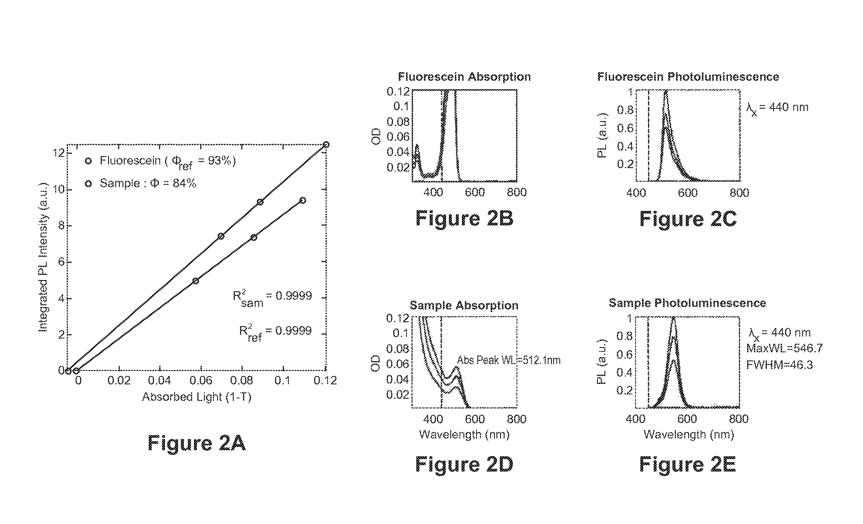
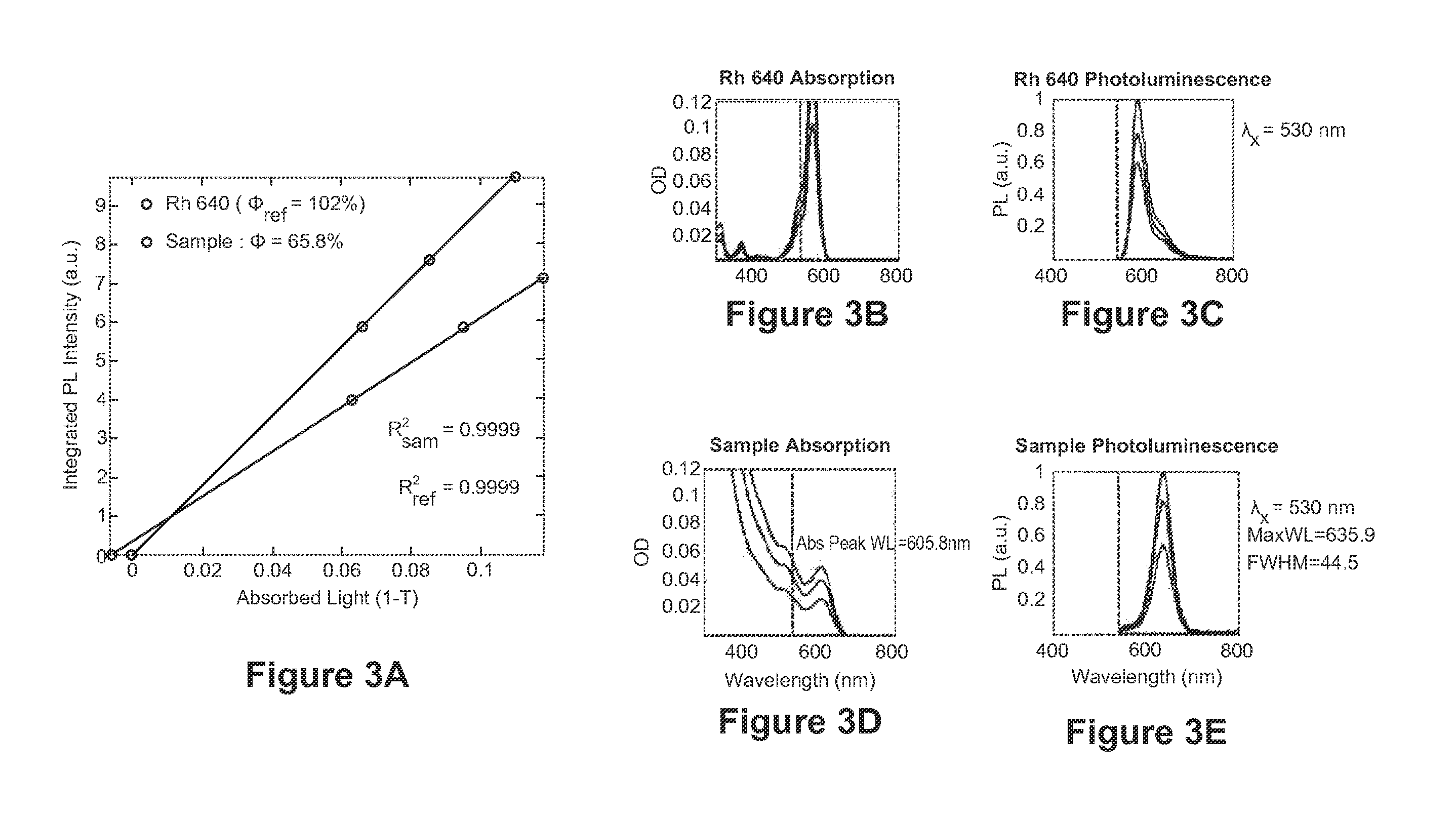
This patent describes methods for producing highly luminescent nanostructures with high quantum yields. The methods involve enriching indium nanostructure cores, using certain ligands during shell synthesis, and implementing a two-step growth of a layered shell. The resulting nanostructures have been shown to have significantly improved quantum yields compared to unenriched nanostructures. The thickness of the shell layers can be controlled by adjusting the amount of precursors provided, and indium can be enriched onto InP nanostructures to further enhance their quantum yield.

Problems solved by technology

However, the intrinsic toxicity of cadmium raises environmental concerns which limit the future application of such cadmium-based nanoparticles.
High quantum yield InP nanostructures, however, have been difficult to obtain.

Method used

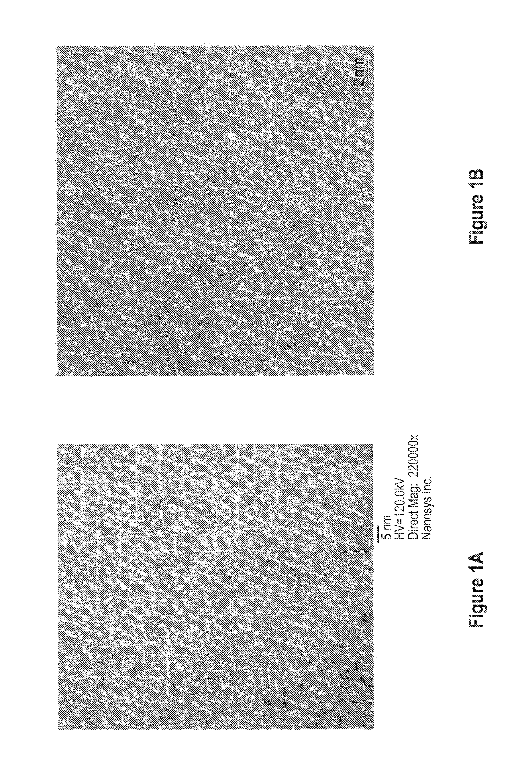

Image

  • Highly luminescent nanostructures and methods of producing same
  • Highly luminescent nanostructures and methods of producing same
  • Highly luminescent nanostructures and methods of producing same

Examples


example 1

Synthesis of Highly Luminescent Quantum Dots

Synthesis of InP Core for Green-Emitting Core / Shell Dots

[0146]To produce the InP cores, 5 g of trioctylphosphine oxide (TOPO), 2.33 g of indium acetate (8 mmol), and 4.797 g of lauric acid (24 mmol) are added to a reaction flask. The mixture is heated to 160° C. for 40 minutes and then 250° C. for 20 minutes under vacuum. The reaction temperature is then increased to 300° C. under N2 flow. At this temperature, 1 g tris(trimethylsilyl)phosphine (4 mmol) in 3 g trioctylphosphine (TOP) is quickly injected into the reaction flask, and reaction temperature is kept at 260° C. After one minute, the reaction is stopped by removing the heating element, and the reaction solution is allowed to cool to room temperature. 8 ml toluene is added to the reaction mixture in the glove box, and the InP dots are precipitated out by addition of 25 ml ethanol to the mixture followed by centrifugation and decantation of the supernatant. The InP dots obtained are ...

example 2

Zinc Sulfide Shell Formation Using an Organic Thiol Sulfur Precursor

[0164]Green-emitting InP cores are synthesized as described above. To achieve indium core enrichment, 25 mg InP cores in solution in hexane, 6 ml ODE, and 0.5 g of indium laurate in ODE (prepared as detailed above) are added to a reaction flask. The mixture is put under vacuum for 10 minutes at room temperature. The temperature is then increased to 230° C. and held at that temperature for 2 hours.

[0165]The reaction temperature is then lowered to 140° C., and 0.7 g hexanoic acid is added to the reaction flask, which is held at 140° C. for 10 minutes. A 0.5 monolayer thick ZnSSe shell is formed by drop-wise addition of 21 mg diethyl zinc, 13 mg bis(trimethylsilyl)selenide, and 10 mg hexamethyldisilthiane in 1 ml ODE to the reaction mixture over 2 min. After ZnSSe precursor addition, the reaction temperature is held at 140° C. for 30 minutes. The temperature is then increased to 200° C. A two monolayer thick ZnS shell ...


PUM

PropertyMeasurementUnit
average diameteraaaaaaaaaa
diameteraaaaaaaaaa

Abstract

Highly luminescent nanostructures, particularly highly luminescent quantum dots, are provided. The nanostructures have high photoluminescence quantum yields and in certain embodiments emit light at particular wavelengths and have a narrow size distribution. The nanostructures can comprise ligands, including C5-C8 carboxylic acid ligands employed during shell formation and / or dicarboxylic or polycarboxylic acid ligands provided after synthesis. Processes for producing such highly luminescent nanostructures are also provided, including methods for enriching nanostructure cores with indium and techniques for shell synthesis.

Description

CROSS-REFERENCE TO RELATED APPLICATIONS[0001]This application is a divisional of U.S. patent application Ser. No. 13 / 917,570, filed Jun. 13, 2013, which claims the benefit of the following prior provisional patent application: U.S. Ser. No. 61 / 667,147, filed Jul. 2, 2012, entitled “HIGHLY LUMINESCENT NANOSTRUCTURES AND METHODS OF PRODUCING SAME” by Wenzhuo Guo et al., which is incorporated herein by reference in its entirety for all purposes.FIELD OF THE INVENTION[0002]The invention pertains to the field of nanotechnology. More particularly, the invention relates to highly luminescent nanostructures, particularly highly luminescent nanostructures comprising an InP core and one or more shell layers. The invention also relates to methods of producing such nanostructures.BACKGROUND OF THE INVENTION[0003]Semiconductor nanostructures can be incorporated into a variety of electronic and optical devices. The electrical and optical properties of such nanostructures vary, e.g., depending on ...

Claims


Application Information

Patent Timeline
Patent Type & Authority Applications(United States)
IPC IPC(8): H01L33/00H01L33/06C09K11/88
CPCH01L33/0083H01L33/06C09K11/883C09K11/02C09K11/565C09K11/70Y10S977/778Y10S977/824Y10S977/825Y10S977/774Y10S977/84Y10S977/818C09K11/025Y10S977/892Y10S977/95B82Y20/00B82Y40/00H01L33/502C09K11/06H01L33/005H01L2933/0025H01L2933/0041
Inventor GUO, WENZHUOCHEN, JIANDUBROW, ROBERTFREEMAN, WILLIAM P.
Owner SHOEI CHEM IND CO LTD
Learn More