P-n junction optoelectronic device for ionizing dopants by field effect

a technology of optoelectronic devices and field effects, which is applied in the manufacture of final products, basic electric elements, and radio frequency controlled devices. it can solve the problems of limiting the efficiency of this type of light-emitting diodes, limiting the efficiency of such a uv led, and the quantity of activated acceptors in algan is then extremely low, so as to achieve improved internal quantum efficiency and improve the effect of emission or detection efficiency

Active Publication Date: 2015-12-31
COMMISSARIAT A LENERGIE ATOMIQUE ET AUX ENERGIES ALTERNATIVES
View PDF15 Cites 43 Cited by
  • Summary
  • Abstract
  • Description
  • Claims
  • Application Information

AI Technical Summary

Benefits of technology

[0008]Thus there is a need to provide a new type of p-n junction optoelectronic device, for example a light-emitting diode or a photodiode, the emission or detection efficiency of which, or the...

Problems solved by technology

The major problem limiting the efficiency of this type of light-emitting diode is the high acceptor activation energy in the p-doped GaN layer, which is typically in the order of 200 meV.
The quantity of activated acceptors in AlGaN is then extremely low, accordingly limiting the efficiency of such a UV LED.
However, the drawback thereof is to limit the radiative efficiency in the active zone of the UV LED which is of ...

Method used


Image

  • P-n junction optoelectronic device for ionizing dopants by field effect
  • P-n junction optoelectronic device for ionizing dopants by field effect
  • P-n junction optoelectronic device for ionizing dopants by field effect

Examples


first embodiment

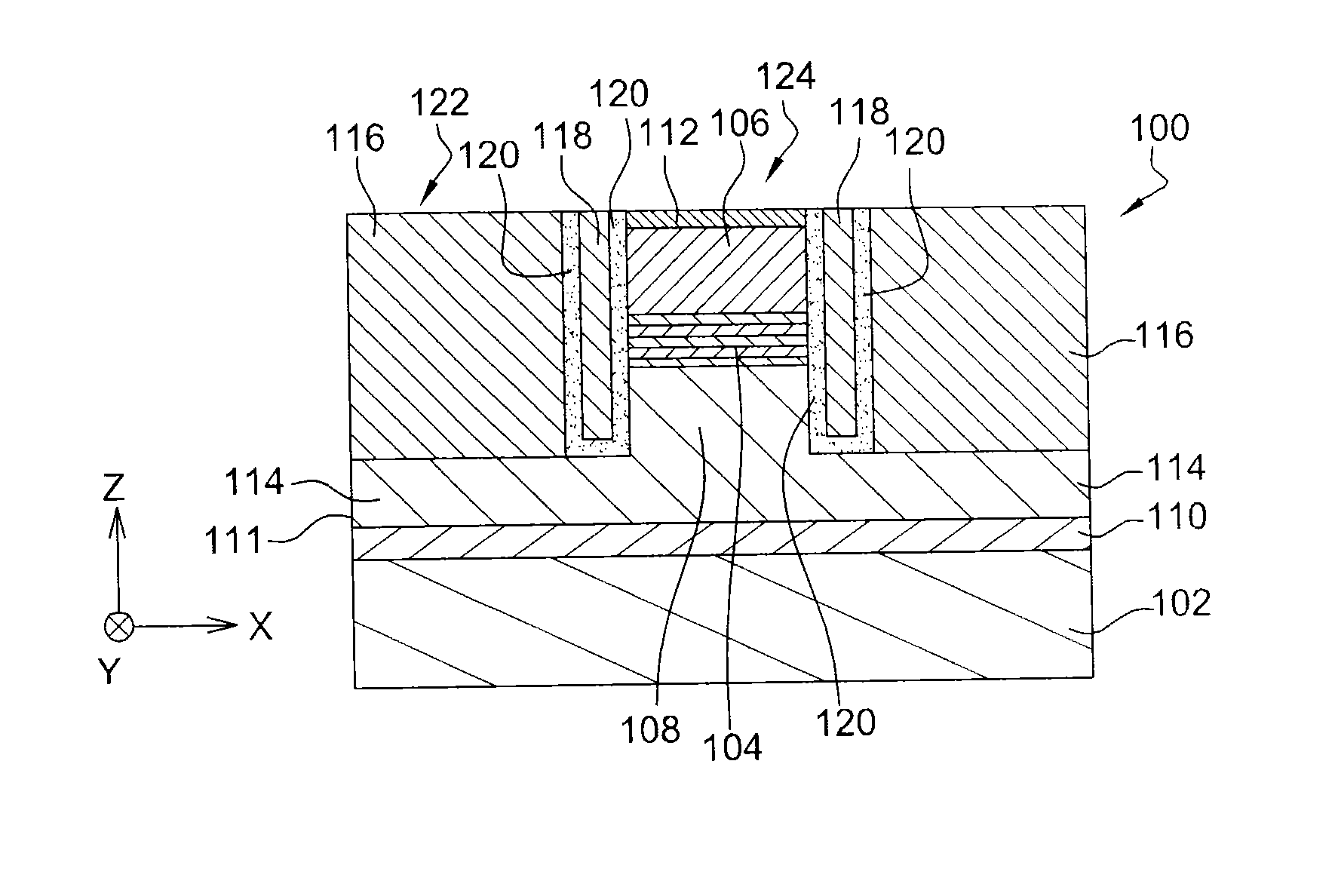
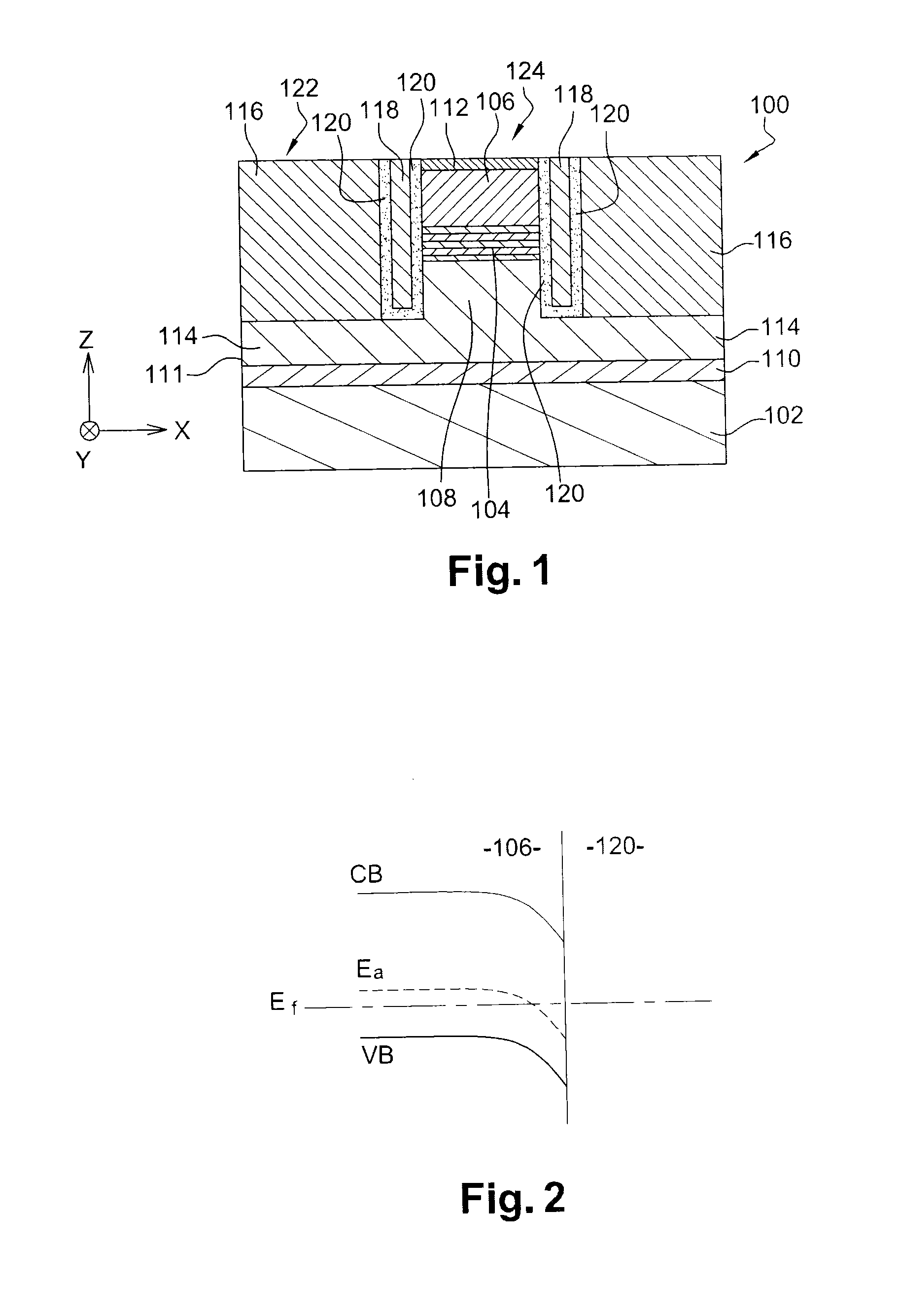
[0101]The LED 100 is made by implementing an etching of a stack of different layers for forming the above described elements of the LED 100. In this first embodiment, the second semiconductor layer 111 forming the second semiconductor portion 108 is not however etched throughout its thickness in order to keep parts 114 of this second semiconductor layer 111 adjacent to the second semiconductor portion 108 so that these n-doped semiconductor parts 114 are electrically connected to a second electrode 116 of the LED 100, which herein corresponds to the cathode since the second portion 108 is n-doped. The second electrode 116 comprises for example a titanium layer with a thickness equal to about 20 nm overlaid by an aluminium layer.

[0102]The second semiconductor layer 111 forming the second semiconductor portion 108 and the parts 114 can be seen as comprising a structured upper face a first protruding part of which forms the second semiconductor portion 108, the second electrode 116 bei...

second embodiment

[0155]FIG. 12 depicts a side cross-section view of an optoelectronic device 100 according to an alternative of the previously described

[0156]In this alternative, a first part 123 of the second semiconductor portion 108 arranged between a second part 125 of the second semiconductor portion 108 and the active zone 104 forms a recess, or an indentation, with respect to the second part 125 of the second semiconductor portion 108. A first part of each of the second electrodes 116 penetrates throughout the second n-doped semiconductor layer 111 as well as the buffer layer 110 and directly rests on the substrate 102. A second part of each of the second electrodes 116 adjacent to the first part rests on an upper face 127 of the second part 125 of the second semiconductor portion 108, and is electrically connected to the second portion 108 of the mesa structure adjacent at this upper face 127. Each of the mesa structures 124a, 124b, and 124c is surrounded by the gate 118 which extends on a s...

third embodiment

[0159]FIGS. 13 and 14 respectively depict a schematic cross-section view (along the axis AA′ depicted in FIG. 14) and a schematic top view of an optoelectronic device 100, here a LED, according to a

[0160]The DEL 100 comprises a single mesa structure 124 which, in the example of FIGS. 13 and 14, has a substantially rectangular shape section, in the plane (X, Y), and is formed by the same layers of materials as those forming the mesa structure 124 of the LED 100 according to the first embodiment.

[0161]In this third embodiment, the mesa structure 124 is not surrounded by the gate 118 but is penetrated by several electrically conductive material portions 118a-118e (5 portions in the example of FIGS. 13 and 14) extending in the mesa structure 124 and forming together the gate 118. In the example described here, the portions 118a-118e correspond to rectilinear shaped portions extending in a direction parallel to the substantially plane surface 122 (parallel to the axis Y in FIG. 14). Each...


PUM


Abstract

An optoelectronic device comprising a mesa structure including:
    • a first and a second semiconductor portions forming a p-n junction,
    • a first electrode electrically connected to the first portion which is arranged between the second portion and the first electrode,
    • the device further comprising:
    • a second electrode electrically connected to the second portion,
    • an element able to ionize dopants of the first and/or second semiconductor portion through generating an electric field in the first and/or second semiconductor portion and overlaying at least one part of the side flanks of at least one part of the first and/or second semiconductor portion and of at least one part of a space charge zone formed by the first and second semiconductor portions,
    • upper faces of the first electrode and of the second electrode form a substantially planar continuous surface.

Description

TECHNICAL FIELD AND PRIOR ART[0001]The invention relates to the field of p-n junction optoelectronic devices such as light-emitting diodes (LEDs or micro-LEDs), particularly used for making any LED-based illuminating device (screens, projectors, video walls, etc.), or photodetecting devices such as photodiodes.[0002]A light-emitting diode emitting a blue light generally includes a GaN-based p-i-n junction comprising: a p-doped GaN layer with typically 1019 acceptors / cm3, a non-intentionally doped or intrinsic GaN layer, with typically 1017 donors / cm3 in which InGaN quantum wells are formed, and an n-doped GaN layer with 1019 donors / cm3. The non-intentionally doped layer including quantum wells in which the light emission occurs is called an active zone. An AlGaN electron blocking layer with an aluminium concentration between 8% and 15% and p-doped can be added between the active zone and the p-doped GaN layer, as described in the document. “The influence of acceptor anneal temperatu...

Claims


Application Information

Patent Timeline
IPC IPC(8): H01L27/15H01L33/24H01L33/38H01L31/113H01L31/0352H01L31/0224H01L27/144H01L33/00H01L31/18
CPCH01L27/156H01L33/38H01L31/186H01L31/03529H01L31/022408H01L31/10H01L33/0041H01L31/1136Y02E10/50Y02P70/521H01L27/1443Y02P70/50
Inventor ROBIN, IVAN-CHRISTOPHEBONO, HUBERT
Owner COMMISSARIAT A LENERGIE ATOMIQUE ET AUX ENERGIES ALTERNATIVES
Why Eureka
Try Eureka