Method for Nanowire Cluster Formation

a nanowire and cluster technology, applied in the field of nanowire fabrication, can solve the problems of increasing the tendency of nanowires to collapse during their separation from the template, and increasing the cost of the techniqu

Active Publication Date: 2016-02-04
INTERUNIVERSITAIR MICRO ELECTRONICS CENT (IMEC VZW) +1
View PDF5 Cites 13 Cited by
  • Summary
  • Abstract
  • Description
  • Claims
  • Application Information

AI Technical Summary

Benefits of technology

[0008]Examples of the present disclosure may provide good templates for the fabrication of a cluster of non-collapsed nanowires. The present disclosure also relates to methods for manufacturing such templates, and to providing a cluster of non-collapsed nanowires.

Problems solved by technology

However, a potential issue for such template-based methods is that the higher the aspect ratio of the nanowires, the more they tend to collapse during their separation from the template.
This technique is however relatively expensive as it involves advanced equipment.
Furthermore, this technique is not easily adaptable to large substrate sizes and to industrial-scale manufacturability.
For example, this technique does not appear to be practically usable for large area foil processing such as roll-to-roll (RtR) processing.

Method used


Image

  • Method for Nanowire Cluster Formation
  • Method for Nanowire Cluster Formation
  • Method for Nanowire Cluster Formation

Examples


example 1

Study of the Inter-Channel Distance Dependence on Anodization Potential

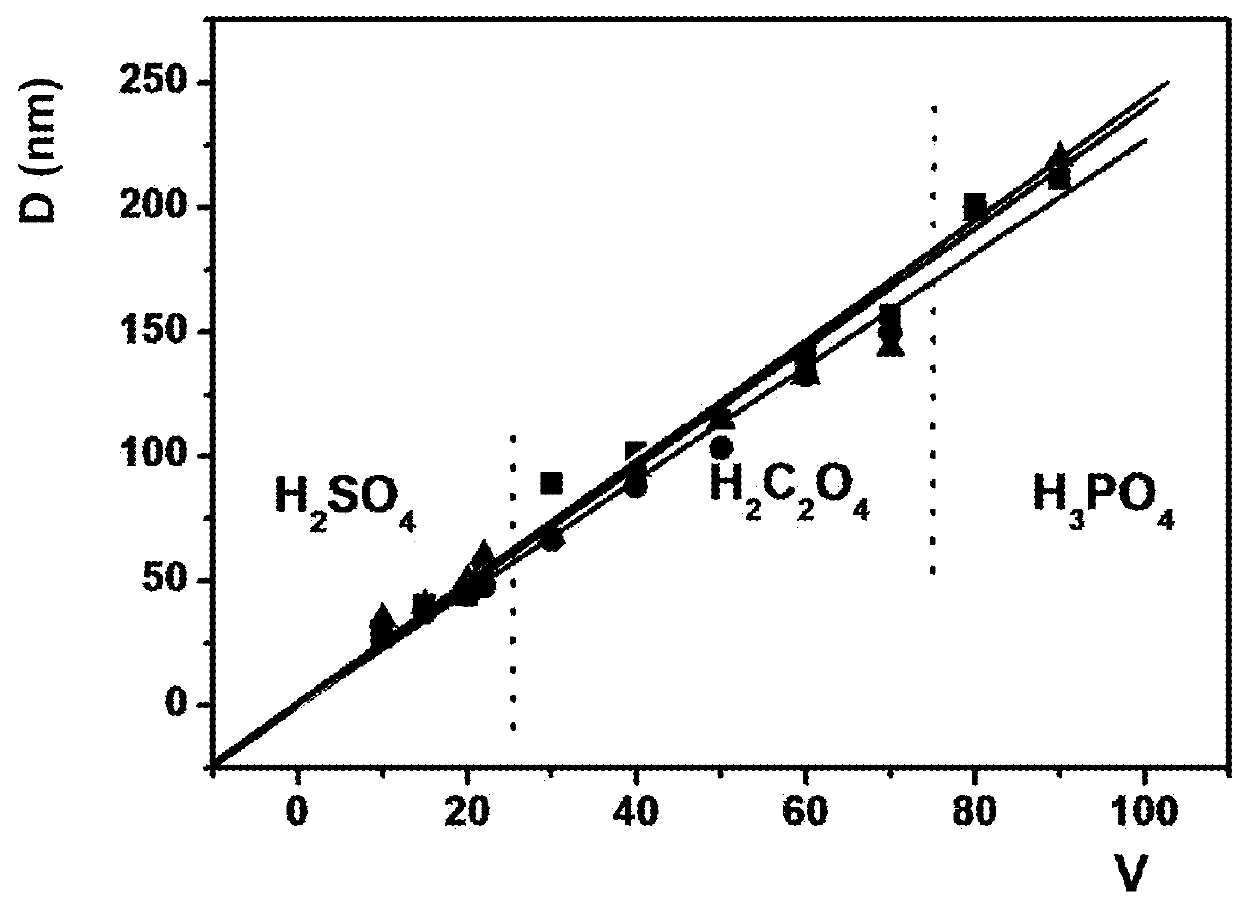
[0100]FIG. 1 shows a graph of the inter-channel distance (nm) versus the anodizing voltage (V) for various anodizable materials. The data points for pure aluminium are represented by squares. The data points for Al doped with 1 wt % Cu are represented by triangles and the data points for Al doped with 1 wt % Si are represented by circles. As can be seen, all three materials behave in a similar way by forming a similar inter-distance at a similar voltage. Small inter-channel distances ranging between 20 and 50 nm were obtained by using H2SO4 as an electrolyte under a voltage of from 10 to about 20V. Inter-distances of from about 50 to 125 nm could be achieved in H2C2O4 under a voltage of from 20 to about 60V. Larger inter-distances up to 225 nm could be achieved in H3PO4 for a voltage up to 90V. Note that higher inter-channel distances can be obtained for even higher voltages which are not shown here.

[0101]The ave...

example 2

Template 16 Construction

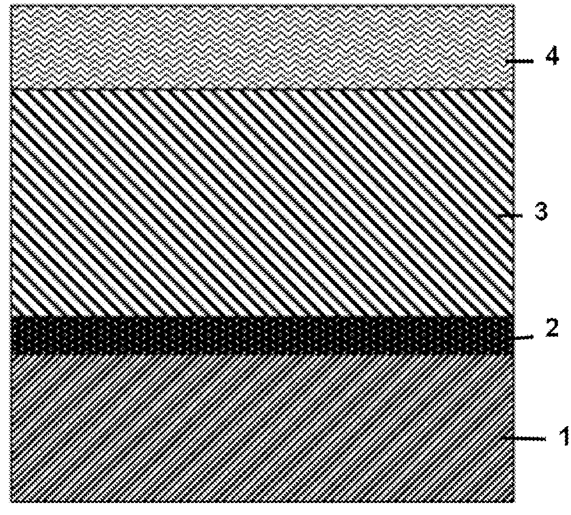
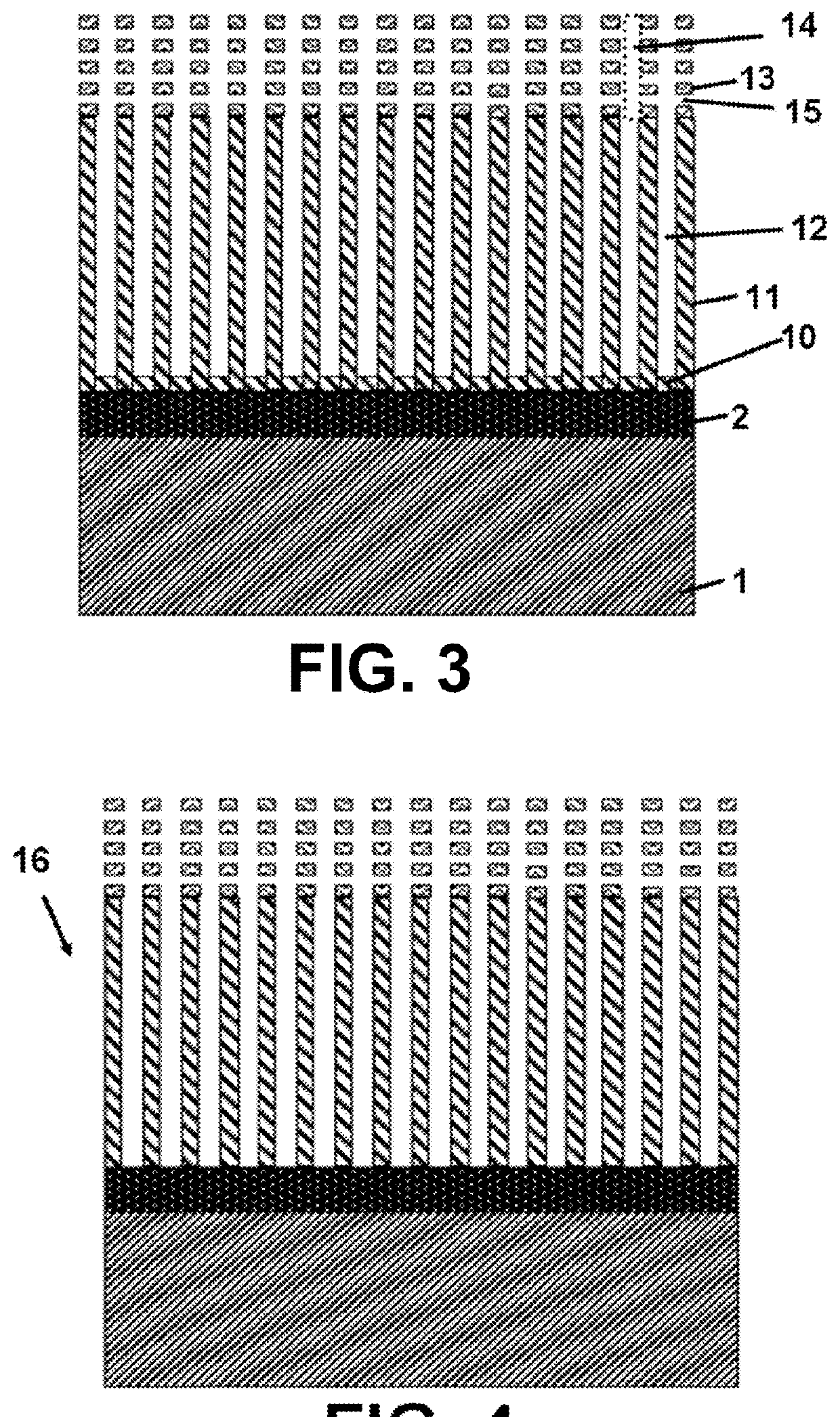
[0103]This process is illustrated in FIGS. 2-4. A silicon wafer 1 (200 mm diameter) coated with 100 nm TiN 2 was provided. A pure aluminium layer 3 (2 μm) was provided thereon by physical vapour deposition (PVD). A 500 nm layer of copper-containing aluminium 4 (0.22 at % Cu) was deposited on the pure aluminium layer 3 by PVD. This bi-layer 3, 4 was connected to the bath 5 of an electrochemical cell 6 as indicated in FIG. 14. The bath 5 was connected to the copper-containing aluminium layer 4 via an O-ring 7 assuring tightness. The bath 5 contained oxalic acid 8 (0.3M) as the electrolyte 8 at room temperature and a Ti counter-electrode 9 (5×3.5 cm Ti sheet 9). The copper-containing aluminium layer 4 was used as the working electrode 4. The so-constructed electrochemical cell 6 was put under potentiostatic control (60V) in order to perform anodization of the bilayer 3, 4. The potential was supplied by an AUTOLAB PGSTAT100 and controlled by a Gpes electrochemica...

example 3

Cluster Formation within the Template 16

[0112]A two-step galvanostatic electrodeposition (ECD) technique was used to fill in the channels 12, 14 and the pores 15 of the template 16 obtained in Example 2, thereby forming nanowires 17 (FIG. 5). It was performed at room temperature and made use of two steps separated by an off period (0A) of 10 s. The first step was with an intensity density of −25 mA / cm2 and lasted 0.1 s. the second step had an intensity density of −5 mA / cm2 and was continued until the fill was completed. The end-point was detected by the observed change in potential and by charge. The reference electrode was an Ag / AgCl / 3M NaCl (0.22 V vs. SHE) electrode. The counter electrode was an inert platinum gauze. The work electrode was the anodized aluminium oxide (AAO) substrate (AAO / TiN / Si). A nickel sulfamate bath (70 g / L nickel sulfamate, 45 g / L boric acid and 3.5 g / L chloride)) was used for the electrodeposition without agitation. After the plating process, the samples w...


PUM

PropertyMeasurementUnit
temperatureaaaaaaaaaa
pore diametersaaaaaaaaaa
diameteraaaaaaaaaa

Abstract

A cluster of non-collapsed nanowires, a template to produce the same, methods to obtain the template and to obtain the cluster by using the template, and devices comprising the cluster are described. The cluster and the template both have an interconnected region and an interconnection-free region.

Description

CROSS-REFERENCE TO RELATED APPLICATIONS[0001]The present application is a non-provisional patent application claiming priority to European Patent Application No. 14179382.8 filed Jul. 31, 2014, the contents of which are hereby incorporated by reference.TECHNICAL FIELD OF THE DISCLOSURE[0002]The present disclosure relates to the field of nanowire fabricationBACKGROUND OF THE DISCLOSURE[0003]In recent years, one-dimensional nanowires have attracted much research interest due to their very large aspect ratio and surface area conferring them with unique magnetic, electronic, and optoelectronic properties. For instance, Au, Ag, Cu and semiconductor nanowires show unique electron transport capabilities, not observed in the corresponding bulk materials; and ferromagnetic nanowires such as Ni, Co and Fe-based nanowires are candidates of choice for magnetic field sensors.[0004]Known methods enabling the fabrication of such nanowires include, for instance, NUR Ubaidah Saidin et al. (Adv. Mat....

Claims


Application Information

Patent Timeline
Patent Type & Authority Applications(United States)
IPC IPC(8): C25D1/00C25D11/04H01B1/02H01B5/00
CPCC25D1/006H01B1/023B82Y40/00C25D11/045H01B5/002B82Y10/00C25D1/20C25D3/12C25D11/005C25D11/24H01L29/0676H01L29/1029H01L29/413H01L29/66439H01L29/66469H01M4/131H01M4/661H01M4/70H01M10/052H01M2004/028Y02E60/10
Inventor HUYGHEBAERT, CEDRICABD-ELNAIEM, ALAAVEREECKEN, PHILIPPE
Owner INTERUNIVERSITAIR MICRO ELECTRONICS CENT (IMEC VZW)
Why Eureka
Try Eureka