Integrated power device with a metal oxynitride active channel for power switching and microwave amplification

a technology of power switching and microwave amplification, which is applied in the direction of pulse generators, amplifiers with min 3 electrodes or 2 pn junctions, pulse techniques, etc., can solve the problems of power amplifiers and low power delivery, and the most difficult one to design and manufacture in si cmos, so as to reduce rf interference and reduce rf interference

Active Publication Date: 2016-04-07
QIU CINDY X +5
View PDF0 Cites 12 Cited by
  • Summary
  • Abstract
  • Description
  • Claims
  • Application Information

AI Technical Summary

Benefits of technology

[0025]FIG. 5b shows a schematic diagram of an integrated power electronic circuit chip (500b) for integration with a power transistor having a low temperature metal oxynitride active channel layer to form an intelligent power switch or an RF amplifier. (500b) includes a thin film capacitor (500Cb) and a thin film resistor (500Rb) disposed of directly on a logic and control circuit chip (410) with a first chip passivation layer (420), a first ground metal layer (422) and a second chip passivation layer (424) to achieve electrical isolation and to reduce RF interferences between the thin film capacitor, thin film resistor and the logic and control circuit chip.
[0026]FIG. 6a shows a schematic diagram of an integrated microstrip transmission line (600) for integration with a power transistor of low temperature metal oxynitride active channel layer to form an intelligent power switch or an RF amplifier. (600) comprises a microstrip transmission line (670) disposed of directly on a logic and control circuit chip (410) with a first chip passivation layer (420), a first ground metal layer (422) and a second chip passivation layer (424) to achieve electrical isolation and to reduce RF interferences between the microstrip transmission line (670) and the logic and control circuit (410).

Problems solved by technology

However, designing and manufacturing wireless transceivers in Si CMOS presents a few challenges.
The most difficult one to design and manufacture in CMOS is the power amplifier.
Thus, transistors have to operate at a lower supply voltage, and therefore delivering low power.
(2) CMOS technology has lower current drive and fmax compared to III-V devices, which means that the gain provided by a single stage is too low and multiple stages are required.
This results in interaction of RF signals with the substrate and causing leakage in a highly integrated CMOS IC.
The leakage from an integrated power amplifier will affect the stability of the IC for example the VCO (voltage controlled oscillator) in a transceiver chain.
Due to the decrease in the line width, gate oxide thickness and junction depth, the breakdown voltage of transistor devices has decreased and this in turn has limited the operating voltage of the MOSFETs.
Therefore it is evident that the power handling capability of conventional MOSFET is not sufficient for switching of high voltage power or generating high power microwaves or millimetre waves.
However, as a result of the reduced junction depth and due to the need to maintain the impurity doping profile in order to retain the performance characteristics of the MOSFET, the thermal budget available for processes after the fabrication of CMOS logic and control circuit chip is limited.
This limitation on thermal budget is also due to the need to maintain the integrity of the metal lines already formed in the CMOS logic and control circuit chip.
This will cause a decrease in the distance between the drain implant region and the source implant region.
Such decrease would lead to a significant variation in output characteristics of the MOSFET and hence that of the logic and control circuits.

Method used


Image

  • Integrated power device with a metal oxynitride active channel for power switching and microwave amplification
  • Integrated power device with a metal oxynitride active channel for power switching and microwave amplification
  • Integrated power device with a metal oxynitride active channel for power switching and microwave amplification

Examples


Embodiment Construction

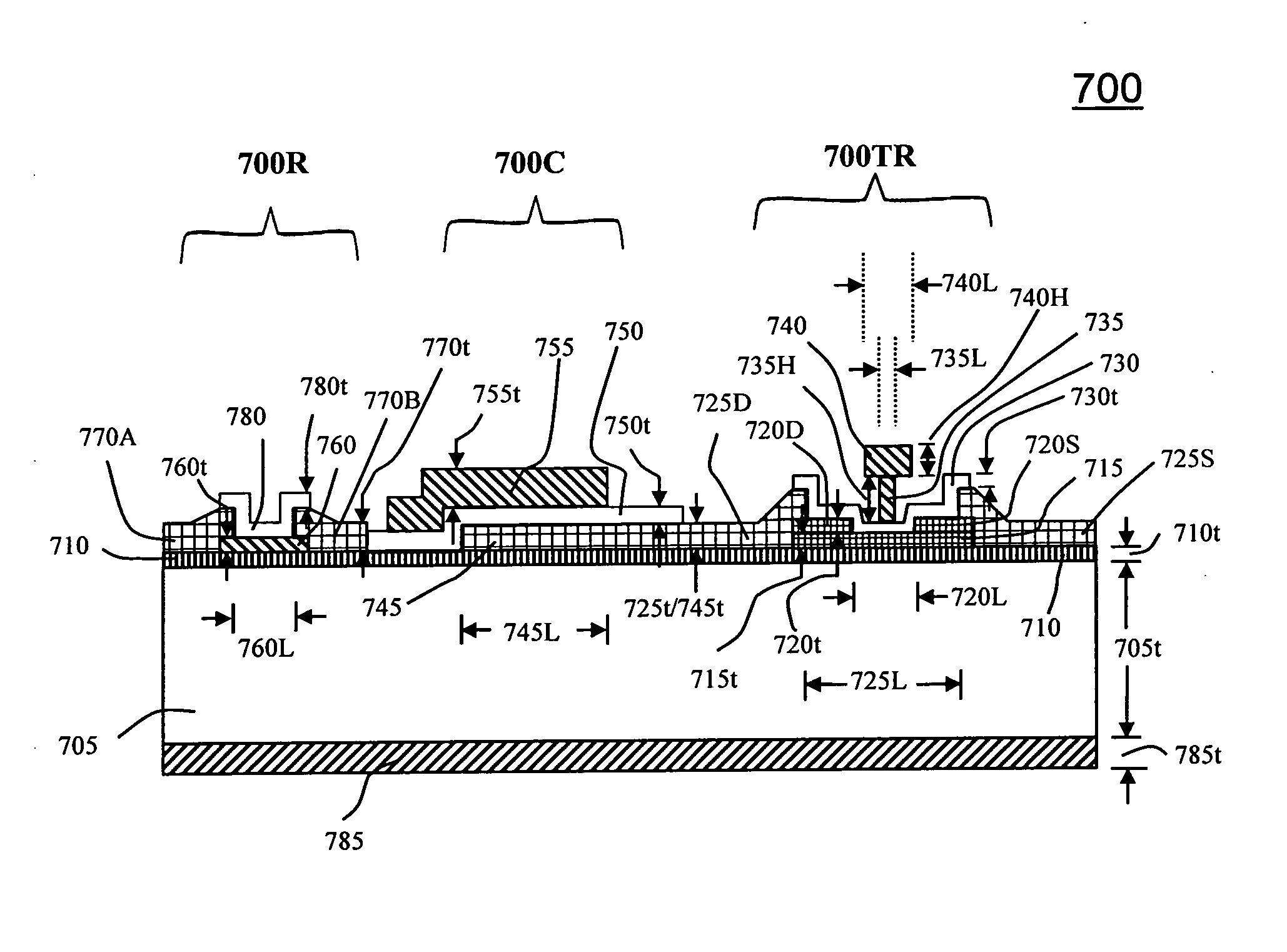
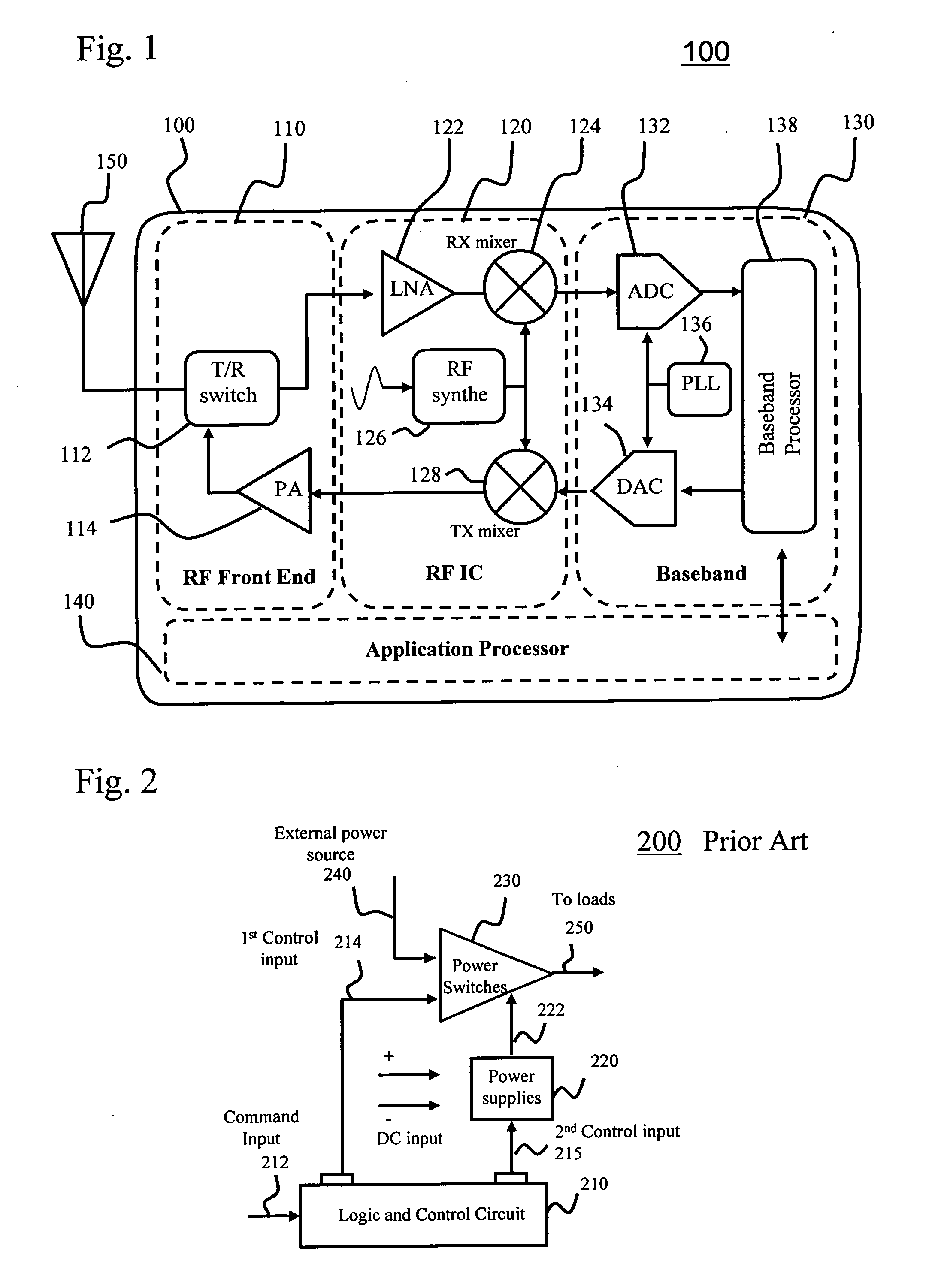
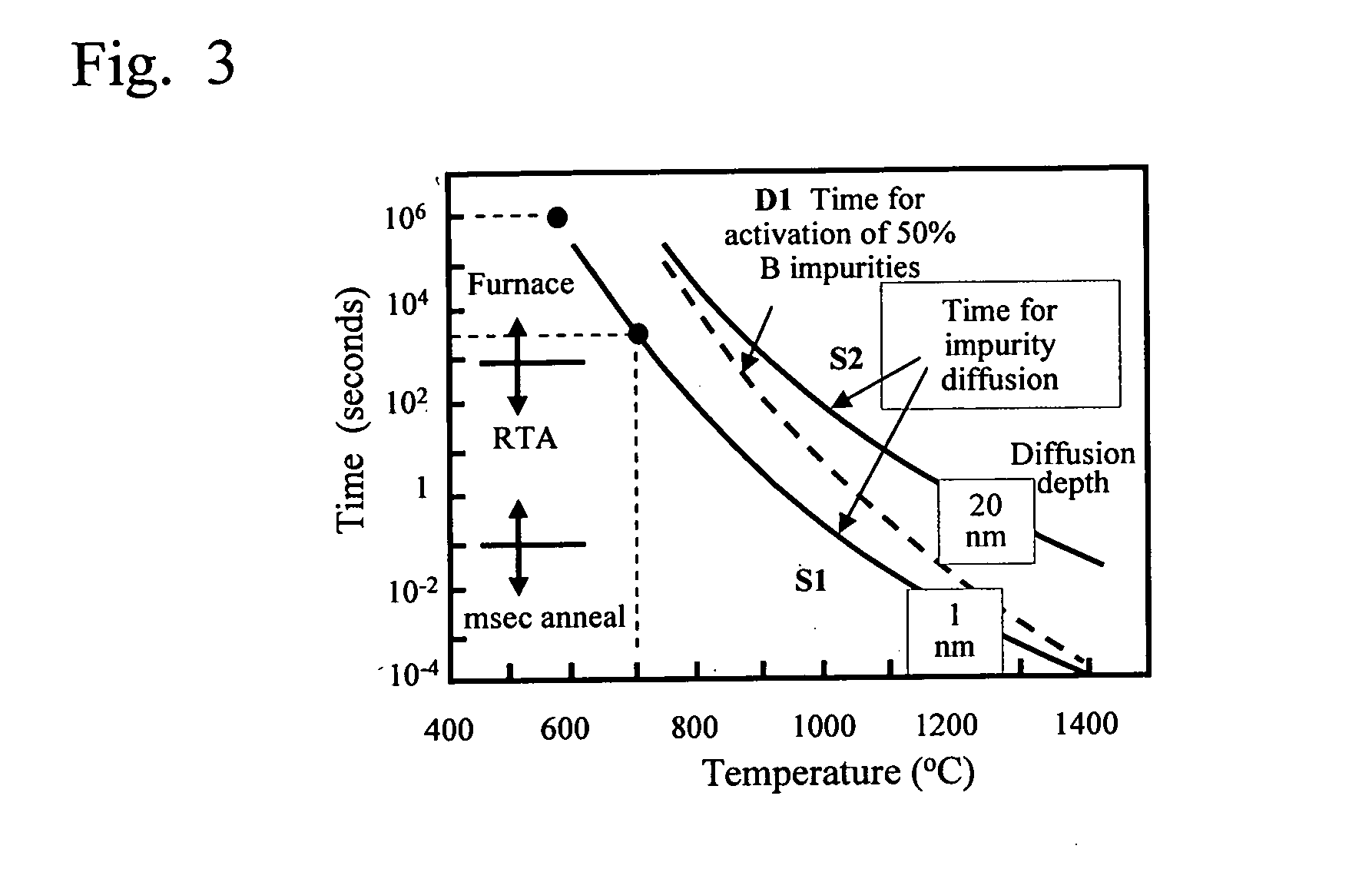
[0029]Transistor devices for electric power switching or for microwave amplification are required to operate at high voltages and / or high frequencies. The operation of these transistor devices is often controlled by a logic and control circuit chip. In order to accomplish an integrated and intelligent power switching and microwave amplification functions, it is preferable to integrate the power transistor devices directly with the logic and control circuit chip. The most convenient logic and control circuits are based on CMOS or BiCMOS on monocrystalline Si due to high degree of integration, capability to implement complex functions and storage. However, as the line width and the deletion region width of the junctions associated with the switches and the amplifiers decrease, the voltage handling level also decreases. This is because the breakdown electric field of monocrystalline Si is substantially a constant, about 3×10⁵ V / cm. The depletion region width of junctions decreases with...


PUM


Abstract

One object of this invention is to provide a structure of integrated power transistor device having low thermal budget metal oxynitrides as the active channel on a CMOS logic and control circuit chip to form an integrated intelligent power switching module for power switching. The other object of this invention is to provide a structure of integrated power amplifier transistor device having low thermal budget metal oxynitride active channel layer on a CMOS logic and control circuit chip to form an integrated intelligent microwave power amplifier for RF power amplification.

Description

FIELD OF THE INVENTION[0001]This invention relates to an integrated power transistor and a power transistor circuit with oxynitride active channel on a CMOS or BiCMOS chip for switching of electrical power and amplification of microwaves.BACKGROUND OF THE INVENTIONIntegrated RF Power Amplifier for Wireless Applications[0002]In wireless communication systems, one of the key components is the RF power amplifier for transmitting and the RF low noise amplifier for receiving at microwave frequencies ranging from 500 MHz to 100 GHz. For mobile handsets, the operating frequencies are usually below 5 GHz. These amplifiers must meet strict performance specifications, output power, noise and linearity so that the wireless systems can meet the performance requirements and regulations. To increase the battery operation time of the current technology, both power-added efficiency (PAE) and the operating voltage must be sufficiently high. In addition, the amplifiers should meet the requirements fo...

Claims


Application Information

Patent Timeline
Patent Type & Authority Applications(United States)
IPC IPC(8): H03F1/02H03K3/012H03F3/195H01L29/20H03F3/213
CPCH03F1/0205H01L29/2003H03F2200/451H03F3/195H03K3/012H03F3/213H01L29/76H01L21/8258H01L27/0688H01L27/1214H01L27/1218H01L27/1255
Inventor QIU, CINDY X.SHIH, ANDYSHIH, YI-CHIHAN, LUQIU, CHUNONGSHIH, ISHIANG
Owner QIU CINDY X
Why Eureka
Try Eureka