Carbon nanotube composite, semiconductor device, and sensor using same

a carbon nanotube and composite technology, applied in thermoelectric devices, instruments, chemistry apparatuses and processes, etc., can solve the problems of difficult control of device variation, limitation of increasing sensitivity, electrical properties, etc., and achieve low cost, high sensing properties, and simple coating process

Inactive Publication Date: 2016-06-02
TORAY IND INC
View PDF3 Cites 15 Cited by
  • Summary
  • Abstract
  • Description
  • Claims
  • Application Information

AI Technical Summary

Benefits of technology

[0016]According to the present invention, a sensor producible at a low cost through a simple coating process and having high sensing properties can be provided.

Problems solved by technology

In the techniques described in Patent Documents 2 and 3, one CNT is used and this makes it difficult to control the variation among devices.
In addition, since a biomolecular recognition substance is disposed on an insulating film and the interaction with a detection substance is detected indirectly, there is a limitation in increasing the sensitivity.
In addition, the insulating dispersant reduces the electrical properties of CNT, and sufficient detection sensitivity can be hardly obtained.

Method used


Image

  • Carbon nanotube composite, semiconductor device, and sensor using same
  • Carbon nanotube composite, semiconductor device, and sensor using same
  • Carbon nanotube composite, semiconductor device, and sensor using same

Examples


example 1

(1) Synthesis of Conjugated Polymer (19)

[0091]6.48 g of iron(III) chloride was dissolved in 30 ml of chloroform, and a chloroform solution (20 ml) containing 1.56 g of 3-thiophenemethyl acetate was added dropwise thereto while stirring under a nitrogen stream. The resulting solution was cooled to 0° C. and after stirring for 24 hours, it was poured in 1 l of methanol. The precipitate was collected and washed with methanol and pure water, and 0.5 g of the solid obtained was added to 50 ml of an aqueous 2.0 M sodium hydroxide solution, followed by stirring at 100° C. for 24 hours. A precipitate resulting from neutralization by the addition of diluted hydrochloric acid was washed with pure water and vacuum-dried at room temperature for 24 hours to obtain Conjugated Polymer (19).

(2) Preparation of Semiconductor Solution

[0092]1.5 mg of CNT1 and 1.5 mg of Conjugated Polymer (19) were added to 15 ml of NMP, and the mixture was ultrasonically stirred at an output of 250 W for 30 minutes by ...

example 2

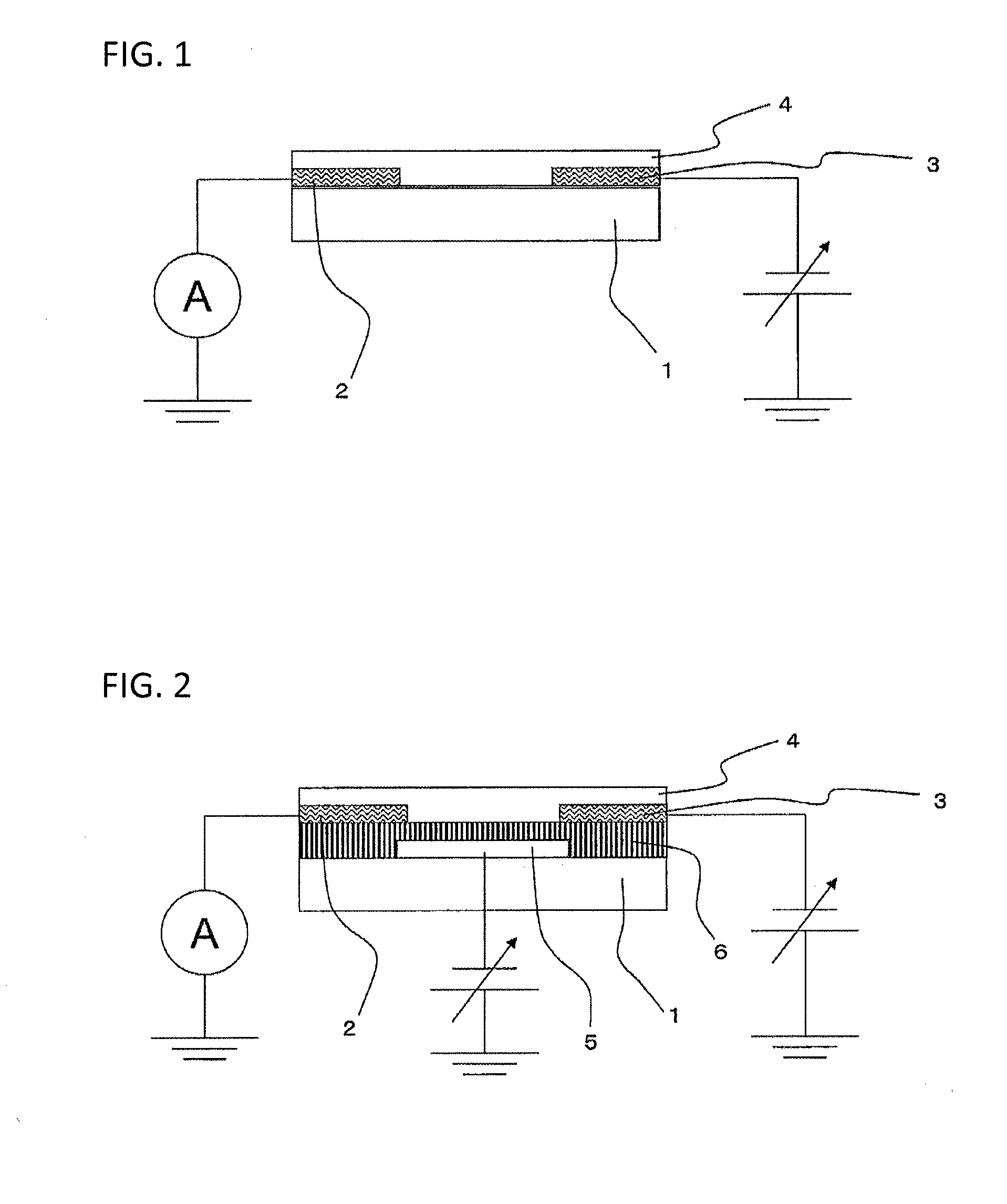
[0101]A sensor in another embodiment was manufactured in the same manner as in Example 1 except that the third electrode 5 and the insulating layer 6 were not formed. The sensor was placed in a measuring box capable of adjusting the atmosphere, and first, the current value flowing between the first electrode 2 and the second electrode 3 was measured in the air and found to be 1.2 μA. Next, an ammonia gas was introduced into the box to have a concentration of 20 ppm, and after a standstill for 5 minutes, the current value was measured, and as a result, the value was greatly changed to 0.7 μA, revealing that the semiconductor device functions as a sensor.

example 3

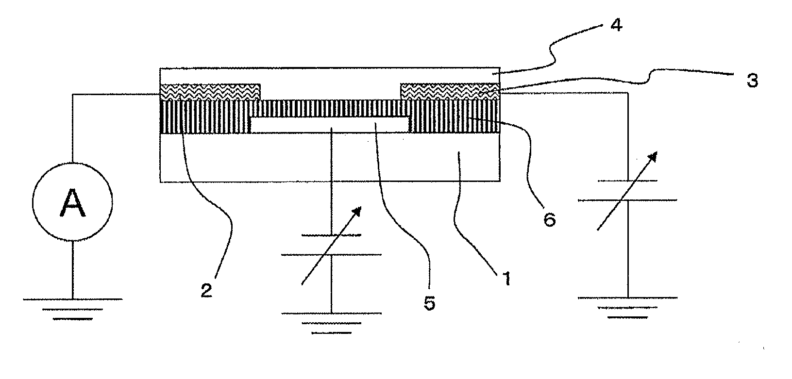
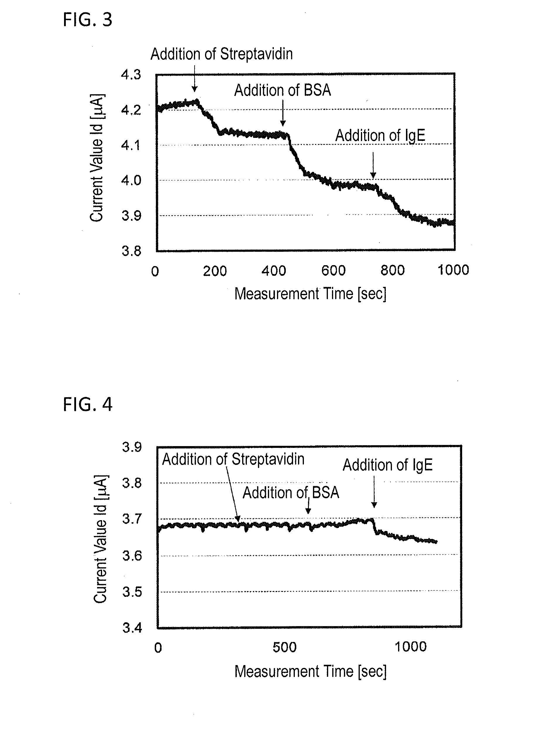
[0102]A semiconductor device was manufactured in the same manner as in Example 1 except that CNT2 was used in place of CNT1. Next, the semiconductor layer 4 of the manufactured semiconductor device was dipped in 100 μl of 0.01 M PBS (pH: 7.2, produced by Wako Pure Chemical Industries, Ltd.), and the current value flowing between the first electrode 2 and the second electrode 3 was measured. The measurement was performed at a voltage (Vsd) between first electrode and second electrode of −0.2 V in the air (temperature: 20° C., humidity: 35%). To the 0.01 M PBS having dipped in the semiconductor layer 4, 20 μl of a 0.01 M PBS solution of streptavidin (produced by Wako Pure Chemical Industries, Ltd.) was added 2 minutes after the start of measurement, 20 μl of a 0.01 M PBS solution of BSA (produced by Aldrich) was added 7 minutes after the start of measurement, and 20 μl of a 0.01 M PBS solution of IgE (produced by Yamasa Corporation) was added 12 minutes after the start of measurement....


PUM

PropertyMeasurementUnit
lengthaaaaaaaaaa
lengthaaaaaaaaaa
diameteraaaaaaaaaa

Abstract

A carbon nanotube composite has an organic substance attached to at least a part of a surface thereof. At least one functional group selected from a hydroxyl group, a carboxy group, an amino group, a mercapto group, a sulfo group, a phosphonic acid group, an organic or inorganic salt thereof, a formyl group, a maleimide group and a succinimide group is contained in at least a part of the carbon nanotube composite.

Description

CROSS REFERENCE TO RELATED APPLICATIONS[0001]This is the U.S. National Phase application of PCT / JP2014 / 069003, filed Jul. 17, 2014, which claims priority to Japanese Patent Application No. 2013-154334, filed Jul. 25, 2013 and Japanese Patent Application No. 2014-079962, filed Apr. 9, 2014, the disclosures of each of these applications being incorporated herein by reference in their entireties for all purposes.TECHNICAL FIELD OF THE INVENTION[0002]The present invention relates to a carbon nanotube composite applicable to sensors such as biosensor, a semiconductor device, and a sensor using the same.BACKGROUND OF THE INVENTION[0003]A semiconductor device such as transistor, memory and condenser is used in various electronics, e.g., a display or a computer, by making use of its semiconductor properties. Development of for example, IC tags or sensors utilizing the electrical properties of a field-effect transistor (hereinafter, FET) is also pursued. Among others, in view of non-necessit...

Claims


Application Information

Patent Timeline
Patent Type & Authority Applications(United States)
IPC IPC(8): H01L51/00G01N27/414C01B31/02C08G61/12
CPCH01L51/0049H01L51/0036C08G61/126G01N27/4146C08G2261/18H01L51/057C08G2261/94C08G2261/72C08G2261/3223C01B31/0273B82Y15/00B82Y30/00C01B32/174Y10S977/746Y10S977/75Y10S977/847Y10S977/932H10K85/225H10K10/488H10K85/113H10K85/761H10K10/84H10K10/491H10K71/10B82Y40/00C08G2261/92
Inventor MURASE, SEIICHIROISOGAI, KAZUKISHIMIZU, HIROJI
Owner TORAY IND INC
Why Eureka
Try Eureka