Direct Electrical Detection of Current-Induced Spin Polarization Due to Spin-Momentum Locking in Topological Insulators

Active Publication Date: 2016-06-16
THE UNITED STATES OF AMERICA AS REPRESENTED BY THE SECRETARY OF THE NAVY
View PDF4 Cites 10 Cited by
  • Summary
  • Abstract
  • Description
  • Claims
  • Application Information

AI Technical Summary

Benefits of technology

[0008]This invention demonstrates a method to directly electrically generate spin polarization due to spin-momentum locking of the topologically protected surface states in topologic

Problems solved by technology

However, attempts at accessing the spin-momentum locking of the surface states by electrical means, i.e., generating such spin polarization and directly

Method used


Image

  • Direct Electrical Detection of Current-Induced Spin Polarization Due to Spin-Momentum Locking in Topological Insulators
  • Direct Electrical Detection of Current-Induced Spin Polarization Due to Spin-Momentum Locking in Topological Insulators
  • Direct Electrical Detection of Current-Induced Spin Polarization Due to Spin-Momentum Locking in Topological Insulators

Examples


example 1

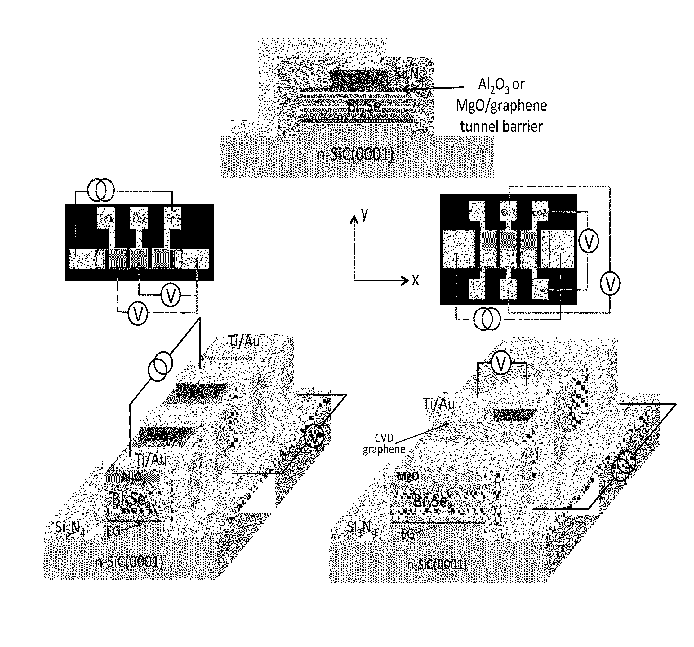
[0024]Briefly, single-crystalline Bi2Se3 thin films are grown by molecular beam epitaxy (MBE). The ferromagnet / oxide tunnel barrier contacts are then grown on top of the Bi2Se3 in separate deposition systems. The samples are then patterned into electrically addressable test structures.

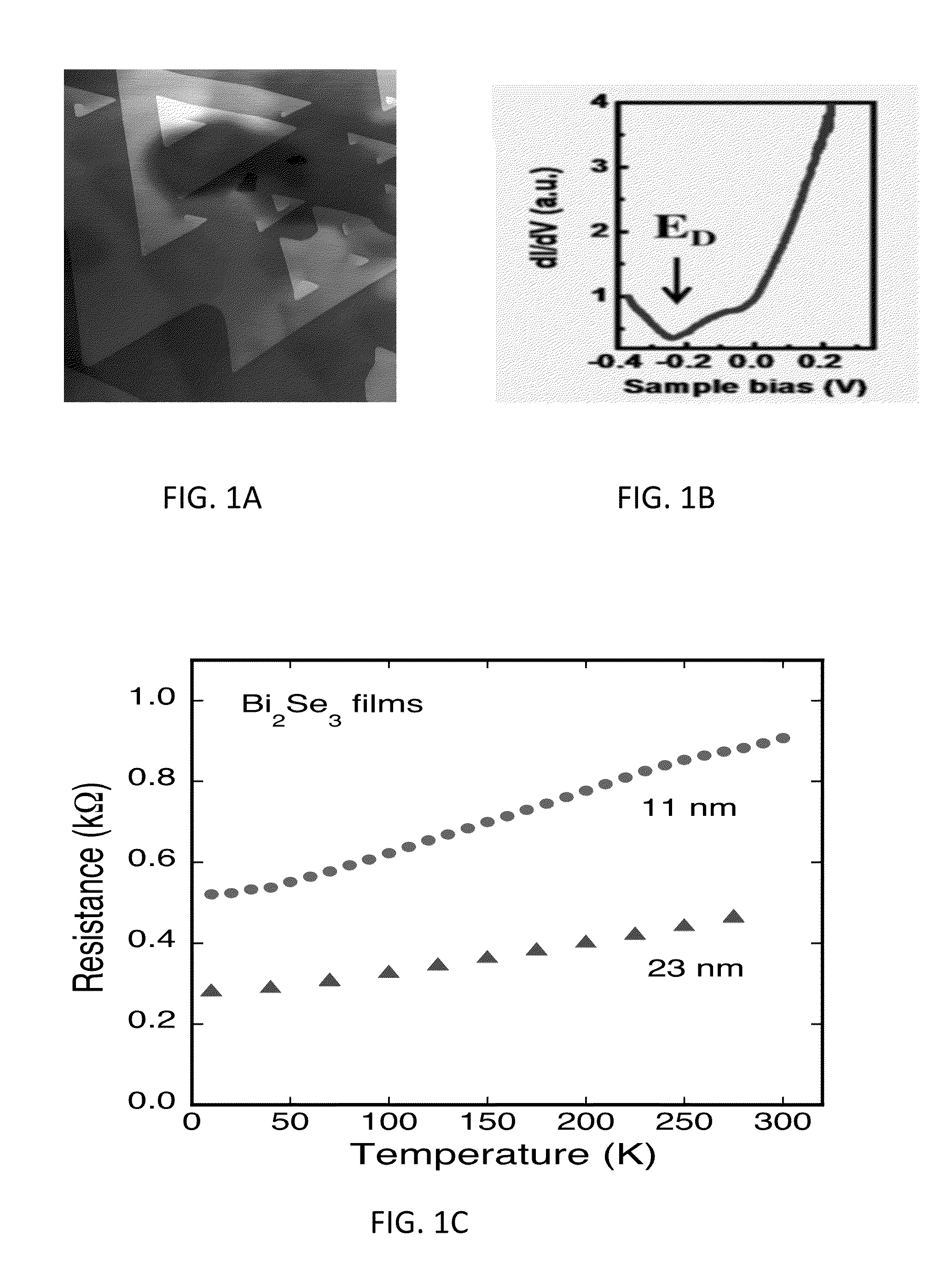
[0025]In situ scanning tunneling microscopy (STM) imaging and tunneling microscopy is used to monitor surface morphology and electronic structure and ensure optimal layer-by-layer spiral growth (FIG. 1) during MBE and film quality (before ferromagnetic / oxide tunnel barrier growth). The as-grown Bi2Se3 film exhibits a Dirac point (ED) 250 meV below the Fermi level in tunneling spectra, indicating n-type doping typically seen in MBE grown materials due to Se vacancies. The as-grown films exhibit n˜1019 / cm3 electron doping, with the Fermi level well within the bulk conduction band, as evident from the metal-like temperature dependent resistance (FIG. 1).

example 2

Deposition of Ferromagnet (FM) / Tunnel Barrier Contact

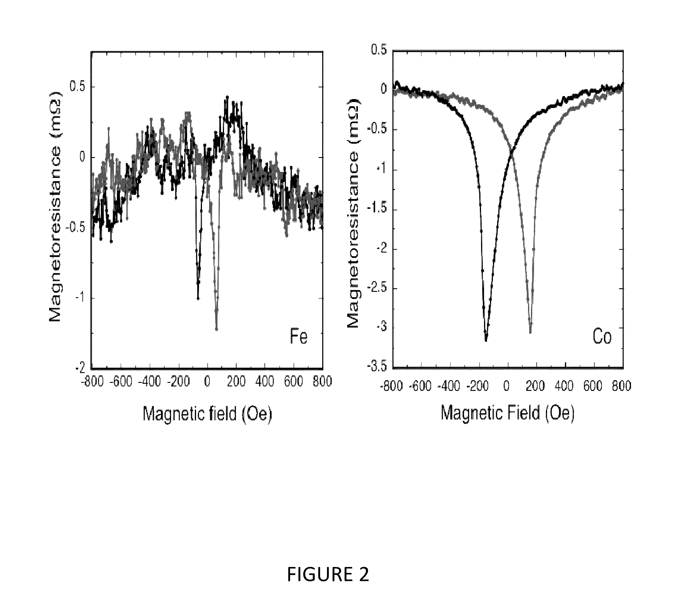
[0026]Two types of FM / tunnel barrier detector contacts are demonstrated as spin sensitive probes. Such contacts have successfully enabled electrical detection of spin current and accumulation in both semiconductors and metals.

[0027]Fe / Al2O3 contacts are deposited on air-exposed Bi2Se3 surface in a separate MBE system as follows. A 0.7 nm layer of polycrystalline Al was first deposited by MBE, and then oxidized in 200 Torr O2 for 20 min in the presence of UV light in the load-lock chamber. This step was then repeated for a total Al2O3 thickness of 2 nm. The sample was then transferred under ultra high vacuum to an interconnected metals MBE chamber, where 20 nm of polycrystalline Fe was deposited at room temperature from a Knudsen cell.

[0028]The oxide tunnel barrier is essential to prevent potential direct magnetic exchange with the TI surface states, interdiffusion between TI and FM which may result in undesirable alloy formation a...

example 3

Sample Fabrication

[0032]The samples were processed into the device structures illustrated in FIG. 3 to enable transport measurements. Standard photolithography and chemical etching methods were used to define the Fe contacts, which ranged in size from 10×10 μm2 to 80×80 μm2, with adjacent contact separation ranging from 45 to 200 μm. Ion milling was used to pattern the Bi2Se3 mesa.

[0033]Large Ti / Au contacts were deposited by lift-off in an electron beam evaporator as non-magnetic reference contacts and bias current leads. The Fe contacts were capped with 10 nm Ti / 100 nm Au, and bond pads for wire bonded electrical connections are electrically isolated from the Si using 100 nm of Si3N4.


PUM


Abstract

A method for directly electrically generating and detecting spin polarization in topological insulators comprising depositing a first and fourth contact on a layer of Bi2Se3 and applying a current between the contacts, which creates a net spin polarization due to spin-momentum locking. A second (comprising ferromagnet/tunnel barrier) and third contact are deposited for detecting the spin polarization. A device for directly electrically generating and detecting the current-generated spin polarization in topological insulators, comprising a first and fourth contact on a layer of Bi2Se3 and a second contact comprising a ferromagnet/oxide tunnel barrier contact as a detector, and a third contact comprising nonmagnetic metal as a reference contact, a current to the first and fourth contact to produce a net spin polarization, and the spin polarization manifesting as a voltage between the second (magnetic) and third (reference) contacts.

Description

[0001]This application claims priority to and the benefits of U.S. Patent Application No. 62 / 089,950 filed on Dec. 10, 2014, the entirety of which is herein incorporated by reference.BACKGROUND[0002]Topological insulators (TI) form a new quantum phase of solid state matter distinct from the classic dichotomy of metals and insulators. Although the bulk is nominally insulating (forms a band gap), the two dimensional surface bands form a Dirac cone populated by massless fermions. These surface states are topologically protected against disorder scattering and are spin-polarized. Hence TIs are expected to produce new functionalities for a wide range of applications such as low power electronics (owing to dissipationless transport), spintronics (utilizing spin-polarized current), and quantum information technology.[0003]One of the unique and most striking properties is that of spin-momentum locking—the spin of the surface state is locked at right angle to the carrier momentum. This chara...

Claims


Application Information

Patent Timeline
IPC IPC(8): G01R33/09H01L43/08H01L43/12H01L43/02H01L43/10
CPCG01R33/096H01L43/02H01L43/08H01L43/12H01L43/10H10N50/85H10N50/01H10N50/10
Inventor LI, CONNIE H.VAN 'T ERVE, OLAF M. T.ROBINSON, JEREMY T.LIU, YINGLI, LIANJONKER, BEREND T.
Owner THE UNITED STATES OF AMERICA AS REPRESENTED BY THE SECRETARY OF THE NAVY
Why Eureka
Try Eureka