High pixel count short-wave to infrared image sensor

Inactive Publication Date: 2016-06-23
JOHNSON PAUL +1
View PDF0 Cites 11 Cited by
  • Summary
  • Abstract
  • Description
  • Claims
  • Application Information

AI Technical Summary

Benefits of technology

[0007]The present invention combines CMOS read-out integrated circuits (ROICs) and photodiode on active pixel (POAP) technology with lead sulfide colloidal quantum dot (PbS-CQD) detector material. This approach provides sensors and systems that are easily manufacturable with high yields The approach dramatically lowers the cost per pixel, reduces the pixel size, and increases

Problems solved by technology

In recent years, much interest has developed for image sensing the SWIR spectral wavelength region (often defined as the spectral range between 1400 nm to 3000 nm but sometime considered to be the range between 1000 nm to 2700 nm), but cur

Method used


Image

  • High pixel count short-wave to infrared image sensor
  • High pixel count short-wave to infrared image sensor
  • High pixel count short-wave to infrared image sensor

Examples


Embodiment Construction

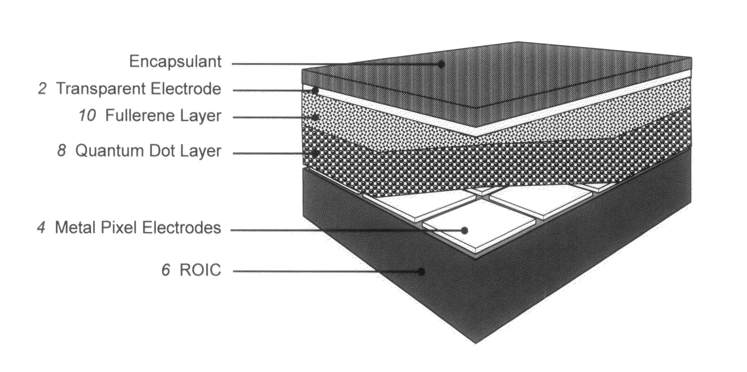
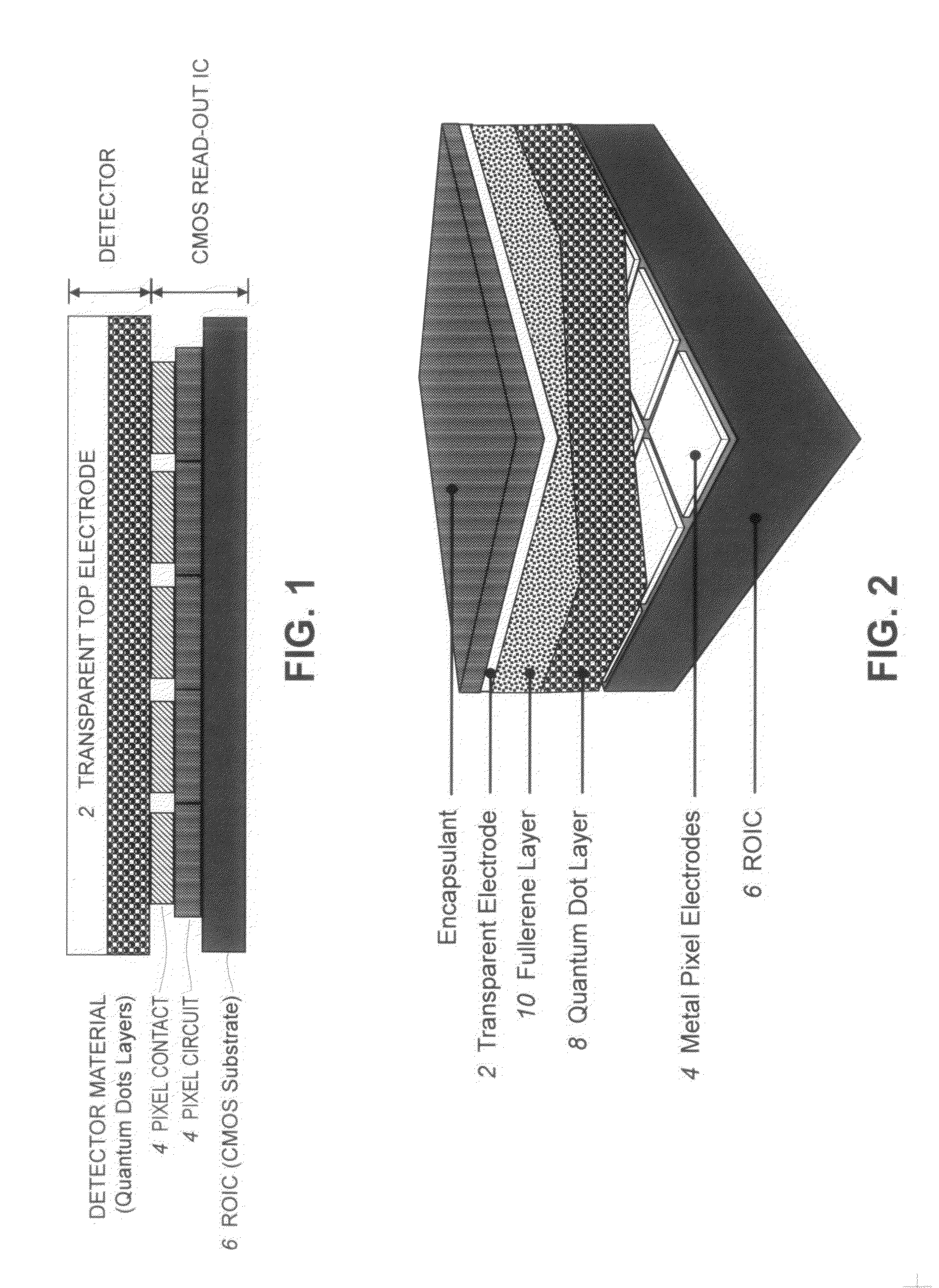
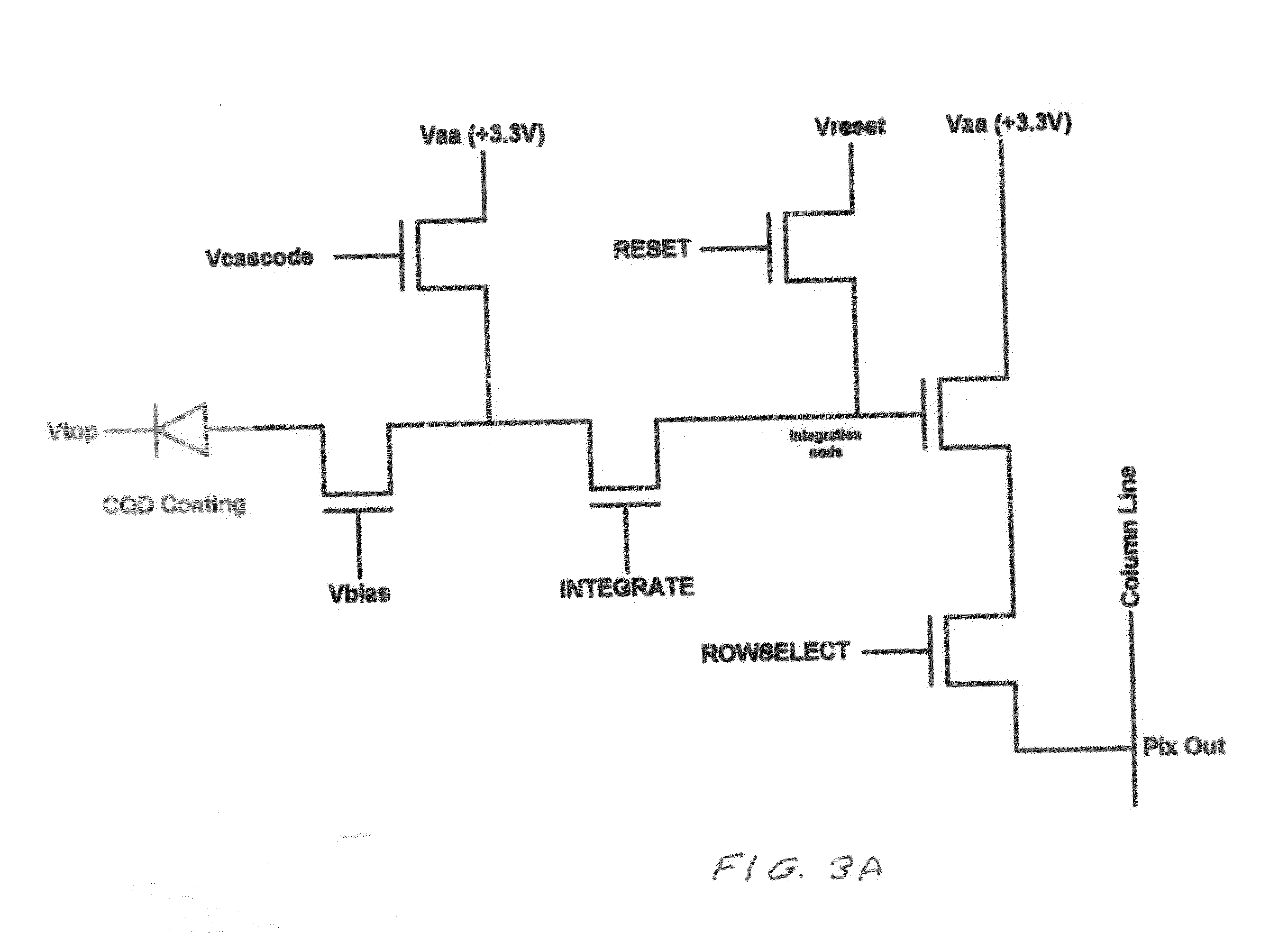
[0019]FIG. 1 illustrates the basic structure of a POAP image sensor, in which a thin film photodetector is applied to the surface of a CMOS readout array. A transparent top electrode 2 provides an electrical bias to the photo-detector top surface relative to pixel electrodes 4 in the ROIC 6. In a preferred embodiment of the invention, a prototype CMOS ROIC has been fabricated in 0.18 μm CMOS process at IBM Microelectronics, though other foundries such as Tower / Jazz, OnSemi, X-Fab, Cypress, and others are capable of producing similar ROICs. In a preferred embodiment, the detector layer is comprised of a multi-layer structure featuring a colloidally suspended Quantum Dot layer 8 as a light absorbing material, and forming a vertical PN diode structure at each pixel as illustrated in FIG. 2. In the preferred embodiment, the Quantum Dot layer 8 is applied to the ROIC by RTI International, Research Triangle Park, N.C., using quantum dots of specific diameter (˜80 nm) to provide good optic...


PUM


Abstract

A CMOS image sensor combining CMOS read-out integrated circuits (ROICs) and photodiode on active pixel (POAP) technology with quantum dot (PbS-CQD) detector material. This approach provides sensors and systems that are easily manufacturable with high yields The approach dramatically lowers the cost per pixel, reduces the pixel size, and increases the pixel count of SWIR sensors and cameras. The PbS-CQD detector material provides optical performance approaching that of InGaAs, and outperforms it in some respects. PbS-CQD detectors include multi-layered conformal thin-films, applied to the ROICs in liquid form. The films are perfectly suited for application over wide surface areas, limited only by wafer or substrate size.

Description

CROSS REFERENCE TO RELATED APPLICATIONS[0001]This application claims the benefit of Ser. No. 61 / 964,124 filed Dec. 23, 2013.FIELD OF THE INVENTION[0002]The present invention relates to imaging sensors and systems and in particular to high pixel count short wave infrared imaging sensors and systems.BACKGROUND OF THE INVENTIONQuantum Dots[0003]A quantum dot crystal is a nanocrystal made of semiconductor materials that are small enough to display quantum mechanical properties. The electronic properties of these materials are intermediate between those of bulk semiconductors and of discrete molecules or atoms. Quantum dots were discovered in the early 1980s. Researchers have studied applications for quantum dots in transistors, solar cells, LEDs, and diode lasers. For example, U.S. Pat. No. 8,742,398 assigned to Research Triangle Institute, Int'l describes photodiodes including layers of Quantum dot material. They have also investigated quantum dots as agents for medical imaging and as ...

Claims


Application Information

Patent Timeline
IPC IPC(8): H01L27/30H01L51/42
CPCH01L27/307H01L51/0046H01L51/426Y02E10/549H01L27/14649H10K39/32H10K85/211H10K30/10
Inventor JOHNSON, PAULSVERDRUP, LAWRENCE
Owner JOHNSON PAUL
Why Eureka
Try Eureka