Silicon-containing polymer, silicon-containing compound, composition for forming a resist under layer film, and patterning process

a technology of silicon-containing compound and composition, which is applied in the field of silicon-containing polymer, silicon-containing compound, composition for forming silicon-containing resists under layer films, and patterning processes, can solve the problems of change of optical systems, high cost of scanners, and extremely poor durability of soft pellicles, and achieve excellent surface roughness, high etching selectivity, and excellent adhesiveness.

Active Publication Date: 2016-08-11
SHIN ETSU CHEM IND CO LTD
View PDF18 Cites 7 Cited by
  • Summary
  • Abstract
  • Description
  • Claims
  • Application Information

AI Technical Summary

Benefits of technology

[0039]As mentioned above, when a resist under layer film formed from a composition that contains the silicon-containing polymer or the silicon-containing compound of the present invention is used, the formed resist pattern becomes excellent in adhesiveness, and a pattern having excellent surface roughness can be formed without pattern collapse in both alkaline development (positive development) and organic solvent development (negative development). Further, since this resist under layer film has high etching selectivity relative to an organic material, the formed photoresist pattern can be successively transferred to the silicon-containing resist under layer film and the organic under layer film or the CVD carbon film by dry etching process. Especially, as the manufacturing process of a semiconductor apparatus progresses toward further miniaturization in recent years, the upper resist layer is made thinner in order to prevent pattern collapse after development, which leads to difficulty in pattern transfer to the under layer film. However, when the inventive composition for forming a silicon-containing resist under layer film is used, the pattern can be transferred to the substrate with high precision while suppressing the deformation of the upper resist pattern during dry etching even if a thinned upper resist is used as etching mask.
[0040]In addition, in practical manufacturing process of a semiconductor apparatus, all the patterning processes are not replaced to the negative development, but only a part of an ultrafine process is replaced; and thus, it may be assumed that the conventional positive development process remains unchanged. In this case, if the resist under layer film is solely dedicated to negative development or positive development, the equipment may become complicated and quality control may also become cumbersome. Accordingly, when a composition for forming a silicon-containing resist under layer film usable in both positive and negative processes, like the one in the present invention, is used, rational management is possible in both equipment and quality control.

Problems solved by technology

However, there are many problems in the F2 lithography: cost-up of a scanner due to use of a large quantities of expensive CaF2 single crystal for a projection lens; extremely poor durability of a soft pellicle, which leads to change of an optical system due to introduction of a hard pellicle; decrease in etching resistance of a resist film, and so forth.
Unfortunately, the EUV lithography has problems such as needs for a higher output power of the laser, a higher sensitivity of the resist film, a higher resolution, a lower line edge roughness (LER), a non-defect MoSi laminate mask, a lower aberration of the reflective mirror, and so forth; and thus, there are innumerable problems to be solved.

Method used


Image

  • Silicon-containing polymer, silicon-containing compound, composition for forming a resist under layer film, and patterning process
  • Silicon-containing polymer, silicon-containing compound, composition for forming a resist under layer film, and patterning process
  • Silicon-containing polymer, silicon-containing compound, composition for forming a resist under layer film, and patterning process

Examples


synthesis example 1

Synthesis of Polymer 1

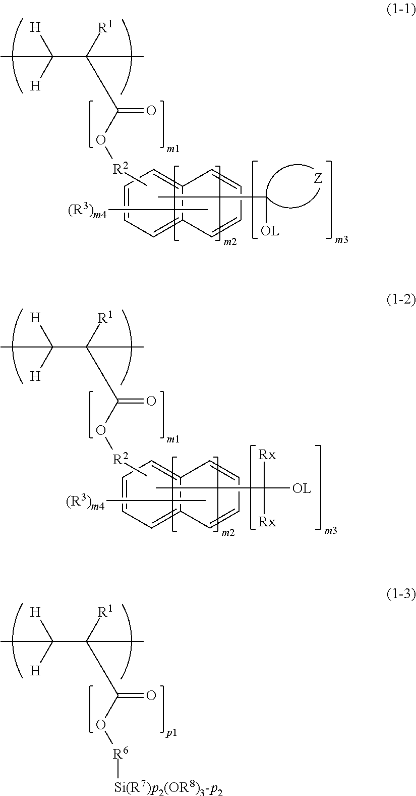
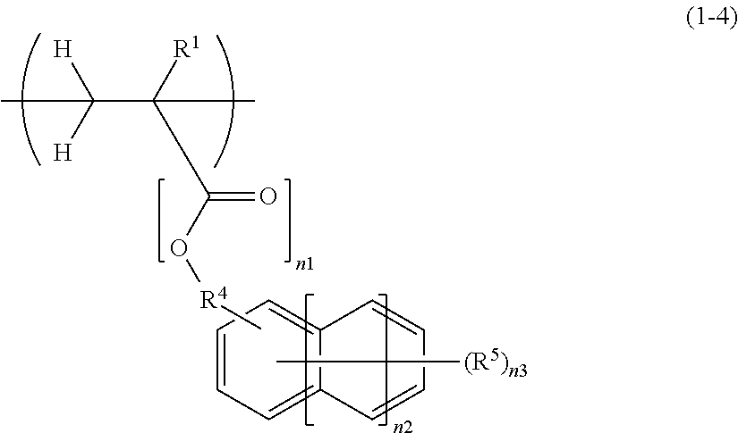
[0168]Into a 200 mL flask was put 14.6 g of propylene glycol monoethyl ether (PGEE) as a polymerization solvent, and heated at 80° C. under nitrogen atmosphere while stirring. 9.73 g (60.0 mmol) of 2-(4-vinylphenyl)-2-propanol [Monomer 1], 8.97 g (40.0 mmol) of 4-(trimethoxysilyl)styrene [Monomer 4], and as a polymerization initiator, a mixture containing 2.30 g of dimethyl-2,2′-azobis(2-methylpropionate) (product name: V601, available from Wako Pure Chemical Industries, Ltd.) and 29.1 g of PGEE were added thereto at 80° C. over 4 hours. After the solution was stirred at 80° C. for 16 hours, the temperature was decreased to room temperature to obtain 64 g of a 32% PGEE solution of Polymer 1 shown by the following structure. The molecular weight in terms of polystyrene and the dispersibility thereof were measured by GPC (Eluent: tetrahydrofuran), consequently finding the following results.

Polymer composition ratio: unit derived from Monomer 1 / unit derived from M...

synthesis examples 2 to 4

Synthesis of Polymers 2 to 4

[0169]The synthesis was performed under the same condition as in Synthesis example 1 by using polymerizable monomers shown in Table 1 to obtain Polymer 2 to Polymer 4 shown in Table 2.

TABLE 1Synthesis examplePolymerizable monomer1Monomer 1: 9.73 g, Monomer 4: 8.97 g2Monomer 2: 17.38 g, Monomer 4: 6.73 g3Monomer 1: 8.11 g, Monomer 5: 10.12 g4Monomer 3: 16.46 g, Monomer 6: 9.29 g

TABLE 2SynthesisMolecular weightDispersibilityexampleProduct(Mw)(Mw / Mn)215,1402.51314,8402.53414,5902.57

Synthesis of Silicon-Containing Polymer (A2)

synthesis example 5

Synthesis of Polymer 5

[0170]Into a 200 mL flask was put 14.6 g of propylene glycol monoethyl ether (PGEE) as a polymerization solvent, and heated at 80° C. under nitrogen atmosphere while stirring. 6.49 g (40.0 mmol) of 2-(4-vinylphenyl)-2-propanol [Monomer 1], 6.73 g (30.0 mmol) of 4-(trimethoxysilyl)styrene [Monomer 4], 5.29 g (30.0 mmol) of 4-tert-butoxystyrene [Monomer 7], and as a polymerization initiator, a mixture containing 2.30 g of V601 and 29.1 g of PGEE were added thereto at 80° C. over 4 hours. After the solution was stirred at 80° C. for 16 hours, the temperature was decreased to room temperature to obtain 64 g of a 32% PGEE solution of Polymer 5 shown by the following structure. The molecular weight in terms of polystyrene and the dispersibility thereof were measured by GPC (Eluent: tetrahydrofuran), consequently finding the following results.

Polymer composition ratio: unit derived from Monomer 1 / unit derived from Monomer 4 / unit derived from Monomer 7=40 / 30 / 30 (molar ...


PUM

PropertyMeasurementUnit
sizeaaaaaaaaaa
wavelengthaaaaaaaaaa
refractive indexaaaaaaaaaa

Abstract

The present invention provides a silicon-containing polymer which contains a repeating unit shown by the general formula (1-3) and one or more repeating units selected from repeating units shown by the general formulae (1-1) and (1-2) as a partial structure. There can be provided a composition for forming a silicon-containing resist under layer film, and a silicon-containing polymer and a silicon-containing compound to give the composition that is capable of forming a resist under layer film improved in adhesiveness in any resist pattern, regardless of negative development or positive development.

Description

BACKGROUND OF THE INVENTION[0001]1. Field of the Invention[0002]The present invention relates to a silicon-containing polymer, a silicon-containing compound, a composition for forming a silicon-containing resist under layer film, and a patterning process using the same.[0003]2. Description of the Related Art[0004]In 1980s, photo-exposure using g-beam (436 nm) or i-beam (365 nm) of mercury lamp as a light source had been widely used in the resist patterning. As a means for finer patterning, shifting to a exposure light having shorter wavelength was assumed to be effective, so that, for the mass production process of DRAM (Dynamic Random Access Memory) with 64 MB (work size of 0.25 μm or less) in 1990s and later ones, KrF excimer laser (248 nm), whose wavelength is shorter than i-beam (365 nm), had been used in place of i-beam as the exposure light source. However, for production of DRAM with integration of 256 MB and 1 GB or higher requiring further finer processing technologies (wor...

Claims


Application Information

Patent Timeline
Patent Type & Authority Applications(United States)
IPC IPC(8): C08F230/08G03F7/40C08L83/14C08F216/10C08F220/20
CPCC08F230/08C08F216/10G03F7/40C08L83/14C08F220/20G03F7/0397G03F7/0751G03F7/0752G03F7/094C08F212/24C08F230/085C08F220/302C08F220/301C08F212/14C08F212/22G03F7/0045G03F7/0758G03F7/039C08F8/12G03F7/11H01L21/0274C08F212/08C08F232/08H01L21/02123C08G77/14C08G77/20
Inventor OGIHARA, TSUTOMUWATANABE, TAKERUMAEDA, KAZUNORI
Owner SHIN ETSU CHEM IND CO LTD
Why Eureka
Try Eureka