
Polishing agent, polishing method and method for manufacturing semiconductor integrated circuit device

a semiconductor integrated circuit and polishing agent technology, applied in the direction of polishing compositions with abrasives, basic electric elements, electric appliances, etc., can solve the problem of insufficient selection ratio between silicon dioxide film and silicon nitride film, insufficient flatness of polishing, and insufficient removal rate of silicon nitride film, etc. problem, to achieve the effect of high removal rate and low removal ra

Active Publication Date: 2016-08-18
ASAHI GLASS CO LTD
View PDF2 Cites 3 Cited by
  • Summary
  • Abstract
  • Description
  • Claims
  • Application Information

AI Technical Summary

Benefits of technology

The present invention aims to provide a polishing agent and method that can effectively remove silicon nitride while maintaining high selectivity towards silicon oxide. This is particularly useful in chemical mechanical polishing (CMP) processes where both silicon oxide and silicon nitride films may be present. The invention helps to achieve a smooth and flat surface, with minimal damage to the underlying substrate.

Problems solved by technology

However, in the polishing agent disclosed in Patent Document 1, high value is secured to a certain degree in a removal rate of a silicon dioxide film, but the suppression of a removal rate of a silicon nitride film is not sufficient.
Therefore, it did not say that the selection ratio between a silicon dioxide film and a silicon nitride film is sufficiently high.
For this reason, flatness of polishing was not sufficient.

Method used


Image

  • Polishing agent, polishing method and method for manufacturing semiconductor integrated circuit device
  • Polishing agent, polishing method and method for manufacturing semiconductor integrated circuit device
  • Polishing agent, polishing method and method for manufacturing semiconductor integrated circuit device

Examples


example 1

[0082]Cerium oxide particles and ammonium polyacrylate having a weight average molecular weight of 5,000 as a dispersant in a mass ratio of 100:0.7 were added to deionized water, and those were mixed by stirring, followed by ultrasonic dispersing and filtering. Thus, a cerium oxide particle dispersion having a concentration of the cerium oxide particles of 10% and a concentration of the dispersant of 0.07% (hereinafter referred to as a “cerium oxide dispersion A”) was prepared. The average secondary particle size of the cerium oxide particles was 0.19 μm.

[0083]Polyether polyamine having a weight average molecular weight of 230 as a water-soluble polyamine (manufactured by BASF, trade name: Polyetheramine D-230) (hereinafter referred to as a “polyetheramine a”), potassium hydroxide and gluconic acid as an organic acid were added to deionized water, and were dissolved therein by stirring and mixing. The resulting solution was mixed with the cerium oxide dispersion A. Thus, a polishing...

example 2

[0084]A solution obtained by adding the polyetheramine a, potassium hydroxide and gluconic acid to deionized water, followed by stirring and mixing was mixed with the cerium oxide dispersion A such that the respective components have the concentrations shown in Table 1, in the same manner as in Example 1. Thus, a polishing agent (2) was obtained. The pH of the polishing agent (2) was 11.3 as shown in Table 1.

example 3

[0085]The polyetheramine a, potassium hydroxide and N-[tris(hydroxymethyl)-methyl]glycine (shown as “tricine” in Table 1) as an organic acid were added to deionized water, and were dissolved therein by stirring and mixing. This solution was mixed with the cerium oxide dispersion A such that the respective components have the concentrations shown in Table 1, in the same manner as in Example 1. Thus, a polishing agent (3) was obtained. The pH of the polishing agent (3) was 11.0 as shown in Table 1.


PUM

PropertyMeasurementUnit
pHaaaaaaaaaa
particle sizeaaaaaaaaaa

Abstract

The present invention relates to a polishing agent including: cerium oxide particles; a water-soluble polyamine; potassium hydroxide; at least one selected from an organic acid and a salt thereof; and water, in which the polishing agent has a pH of 10 or more, a polishing method using the polishing agent, and a method for manufacturing a semiconductor integrated circuit device.

Description

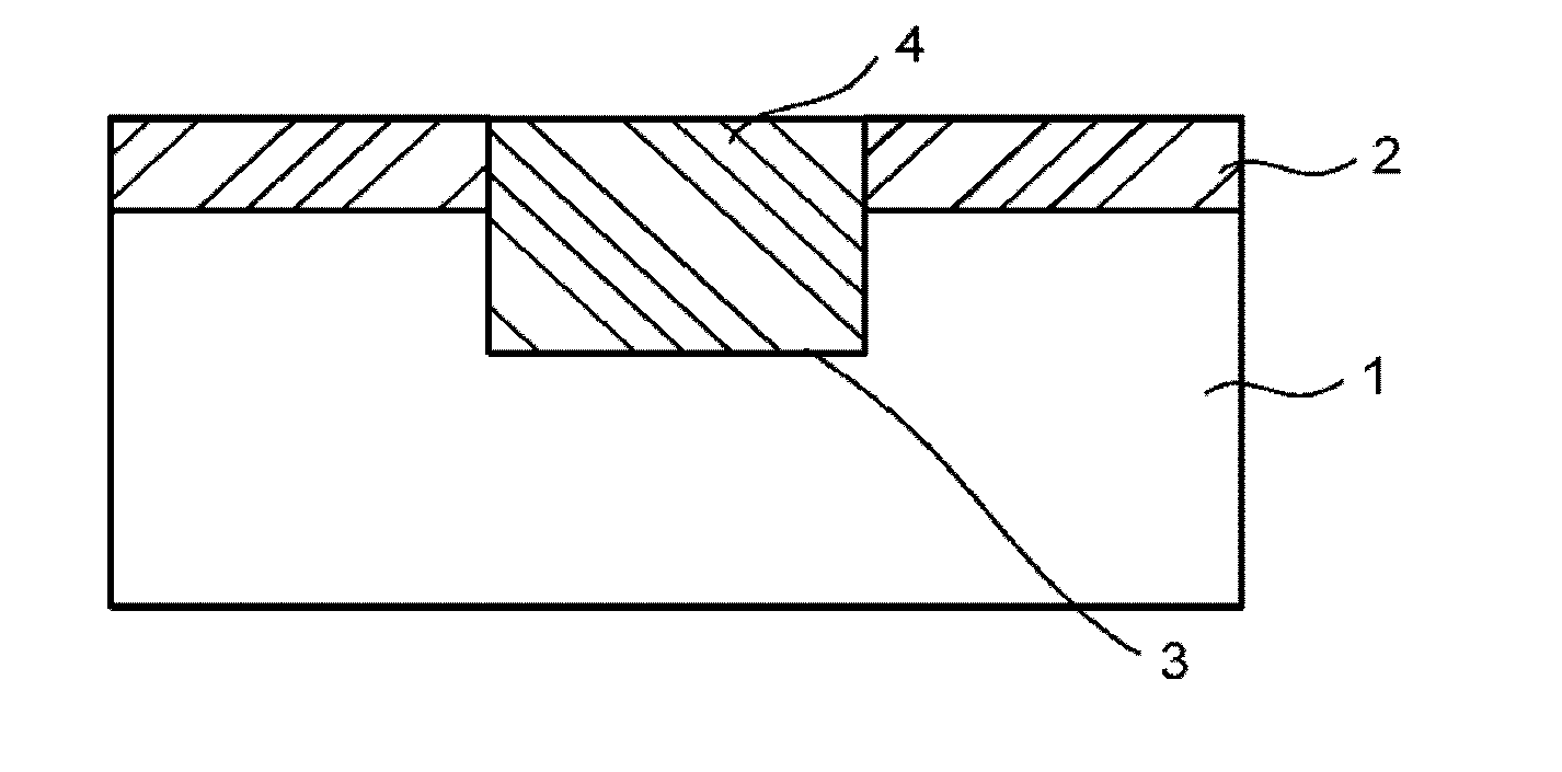
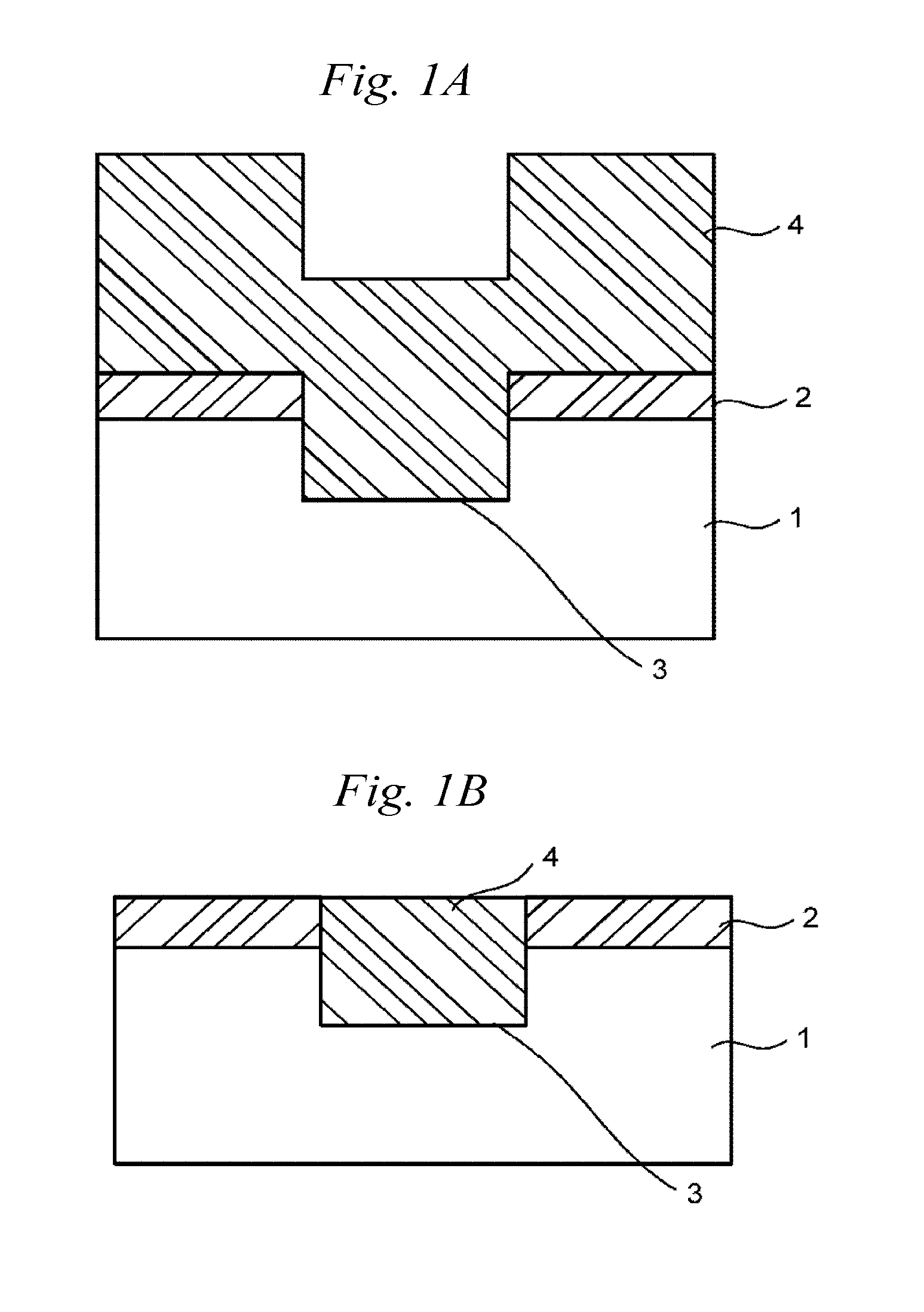
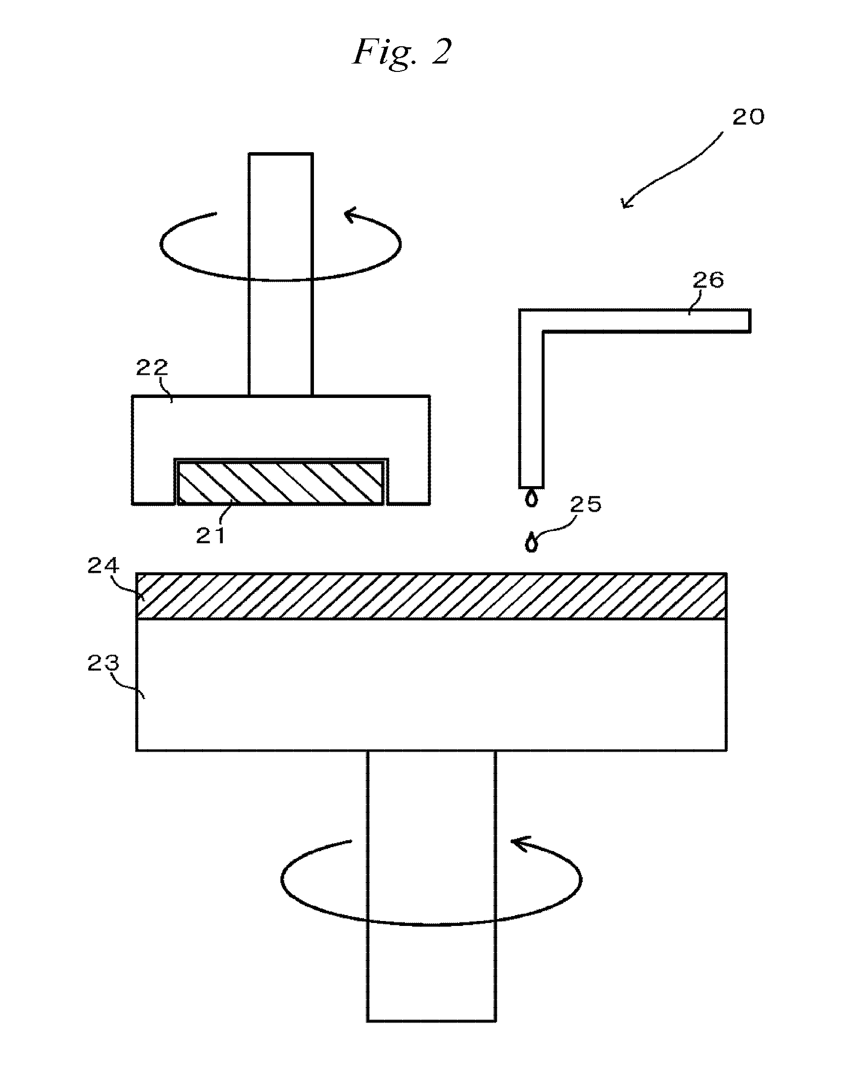
FIELD OF THE INVENTION[0001]The present invention relates to a polishing agent, a polishing method, and a method for manufacturing a semiconductor integrated circuit device. Particularly, the present invention relates to a polishing agent for chemical mechanical polishing in the manufacturing of a semiconductor integrated circuit, a polishing method using the polishing agent, and a method for manufacturing a semiconductor integrated circuit device.BACKGROUND OF THE INVENTION[0002]In recent years, with high integration and high functionality of a semiconductor integrated circuit, the development of microfabrication technology for miniaturization and density growth of a semiconductor element is advancing. In the manufacturing of a semiconductor integrated circuit device (hereinafter also referred to as a “semiconductor device”), in order to prevent the problem such that unevenness (difference in level) of the surface of a layer exceeds depth of focus of lithography and sufficient reso...

Claims


Application Information

Patent Timeline
Patent Type & Authority Applications(United States)
IPC IPC(8): C09G1/02H01L21/3105
CPCH01L21/31053C09G1/02
Inventor SUZUKI, MASARUOTSUKL, TOSHIHIKO
Owner ASAHI GLASS CO LTD
Learn More