Application of electron-beam induced plasma probes to inspection, test, debug and surface modifications

a plasma probe and electron beam technology, applied in the field of nonmechanical contact probes of electronic devices, can solve the problems of high system cost, high system cost, and device damage caused by laser beams

Inactive Publication Date: 2016-10-13
ORBOTECH LTD +1
View PDF0 Cites 12 Cited by
  • Summary
  • Abstract
  • Description
  • Claims
  • Application Information

AI Technical Summary

Benefits of technology

[0024]In any of the disclosed embodiments, the ambient gas may comprise air or a mix of one or more inert gasses. Also, transmitting the electron beam from the vacuum enclosure may comprise passing the electron beam via pinhole provided in an aperture plate separating the vacuum environment from the ambient gas. Transmitting the electron beam from the vacuum enclosure may further comprise passing the electron beam through a membrane prior to passing the electron beam through the pinhole. A voltage potential may be applied to at least one of the sample, the aperture plate or the membrane. The aperture plate or the membrane may comprise a pick-up electrode. The methods may further comprise the use of electron beam and / or plasma for sensing before interaction with or modifying the sample; then processing, interacting or modifying the sample, then sensing again after the processing, interaction or modifying the sample. As such, the methods establish closed-loop processing (sense-process-sense).

Problems solved by technology

They may roughly be divided into two categories, one category being based on high intensity laser-induced ionization, which presents possible risks of laser-induced damage to the device under tests given the high ionization thresholds, and another category being based on high voltage corona discharges, in which ionized species have a wide range of scattering angles (little directional control) and also presents damage risks, especially related to arcing.
This technology involves large vacuum enclosures and complex electron optics, leading to high system costs, large factory foot prints and potentially impacting throughput.

Method used


Image

  • Application of electron-beam induced plasma probes to inspection, test, debug and surface modifications
  • Application of electron-beam induced plasma probes to inspection, test, debug and surface modifications
  • Application of electron-beam induced plasma probes to inspection, test, debug and surface modifications

Examples


Embodiment Construction

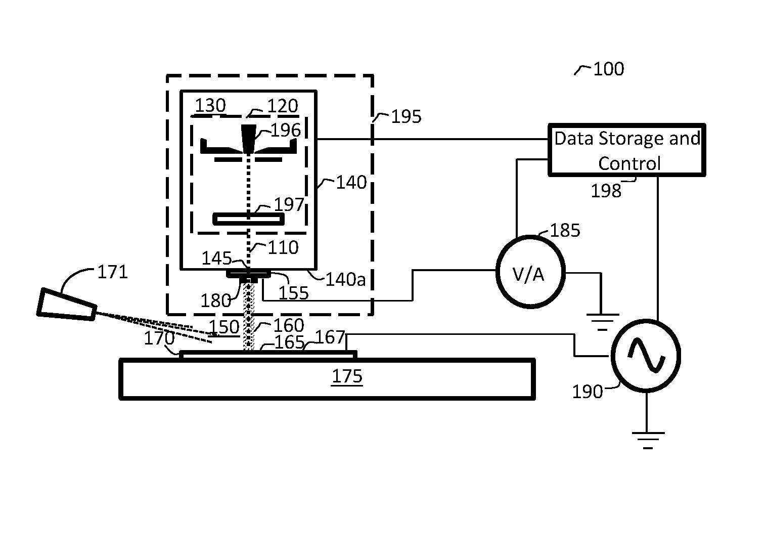
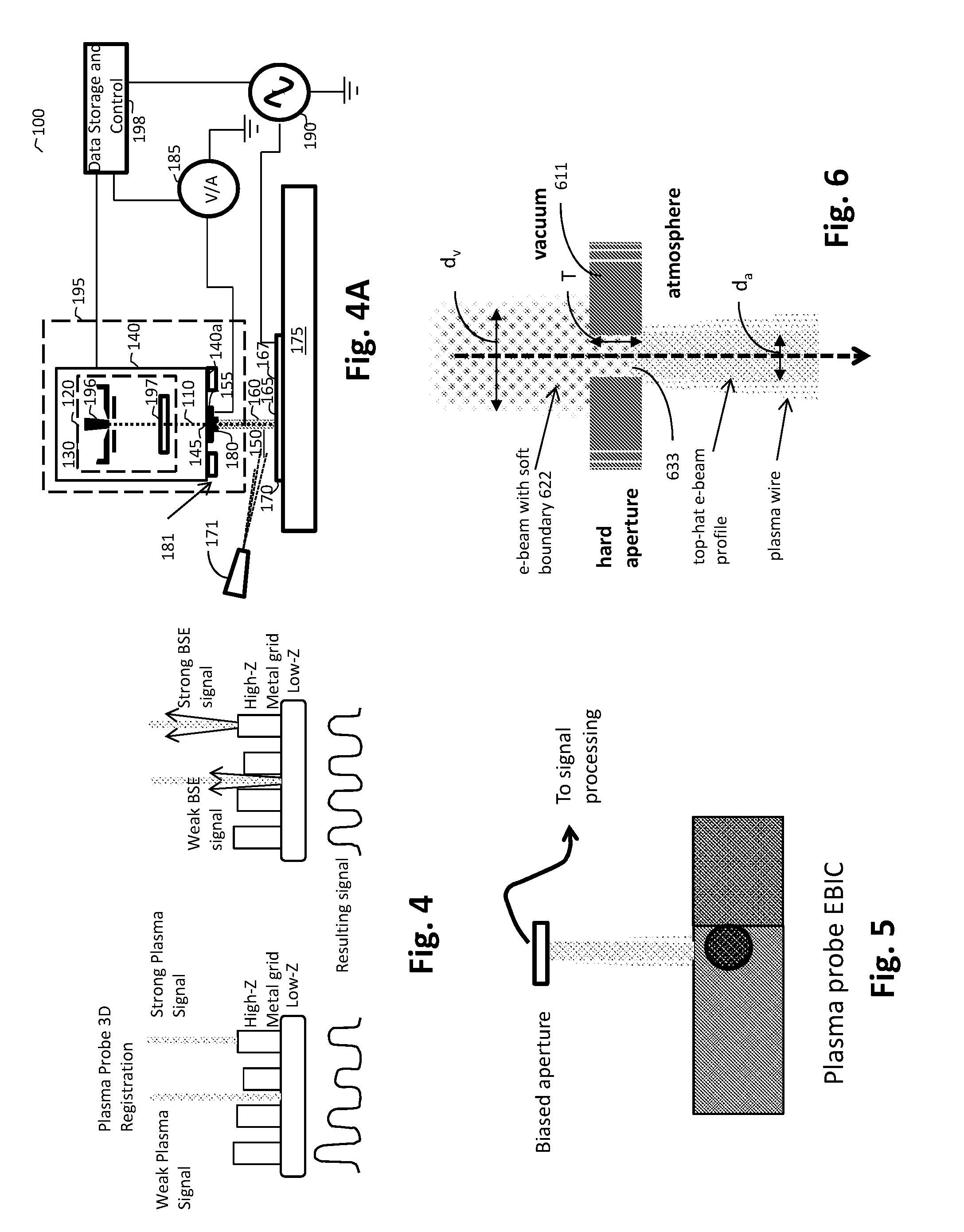
[0040]Various embodiments described below provide solutions based on a high resolution, high sensitivity, and compact atmospheric electron beam induced plasma probe technology. This technology essentially relies on the fact that the cold plasma (a few eV) generated by collisional ionization events driven by the electron beam in air acts as a non-mechanical conductive contact, allowing voltages on the devices under test (DUT) to be measured via the resulting secondary plasma electron current. As implied by the name, this technology does not require the DUT to be held in vacuum. Rather, only the electron emitter (cathode) and electron optics need to be kept in a vacuum enclosure. Furthermore, the implementation of this technology only requires simple electron optics configurations, e.g., an extraction grid and an electrostatic lens, keeping the gun cost low and its size, and hence the size of the enclosure, compact. The electron beam exits the vacuum enclosure containing the electron ...


PUM


Abstract

An electron-beam induced plasmas is utilized to establish a non-mechanical, electrical contact to a device of interest. This plasma source may be referred to as atmospheric plasma source and may be configured to provide a plasma column of very fine diameter and controllable characteristics. The plasma column traverses the atmospheric space between the plasma source into the atmosphere and the device of interest and acts as an electrical path to the device of interest in such a way that a characteristic electrical signal can be collected from the device. Additionally, by controlling the gases flowing into the plasma column the probe may be used for surface modification, etching and deposition.

Description

BACKGROUND[0001]1. Field[0002]Various embodiments of the present invention generally relate to the non-mechanical contact probing of electronic devices and surface modification of devices and tissue. In particular, the various embodiments relate to application of electron-beam induced plasma probes for metrology and surface modification.[0003]2. Related Arts[0004]The ability to measure and apply voltages and currents on patterned structures without having to establish mechanical contact is of importance to the functional (electrical) testing of semiconductor devices and flat panel displays, e.g., liquid crystal and organic light emitting diode (OLED) displays, backplanes, and printed circuit boards, since non-mechanical contact probing minimizes the likelihood of damage to the device / panel under test and is also conducive to improved testing throughput.[0005]Photon Dynamics', an Orbotech company, Voltage Imaging® optical system (VIOS) employs electro-optical transducers to translate...

Claims


Application Information

Patent Timeline
Patent Type & Authority Applications(United States)
IPC IPC(8): G01N27/70H01J37/32
CPCG01N27/70H01J37/3233H01J2237/063H01J37/32825H01J37/32449G01R31/305H01J33/00H01J2237/164H01J2237/188H01J2237/317H05H2240/10H05H2245/40G01R1/072G01R31/2825
Inventor SALEH, NEDALTOET, DANIELSTERLING, ENRIQUELOEWINGER, RONENKRISHNASWAMI, SRIRAMGLAZER, ARIE
Owner ORBOTECH LTD
Why Eureka
Try Eureka