Optically-Finished Thin Diamond Substrate or Window of High Aspect Ratio and a Method of Production Thereof

a technology of diamond substrate and high aspect ratio, which is applied in the direction of chemical vapor deposition coating, metal material coating process, coating, etc., can solve the problems of limited geometrical dimension, limited availability in nature, and inability to meet the requirements of large dimensions,

Active Publication Date: 2016-11-17
II VI DELAWARE INC
View PDF19 Cites 14 Cited by
  • Summary
  • Abstract
  • Description
  • Claims
  • Application Information

AI Technical Summary

Benefits of technology

[0013]The thin diamond substrate or window described herein comprises at least one optically-finished surface and an aspect ratio of 100 or greater, or a combination of a thickness less 400 microns or thinner and a largest geometric dimension of 25 mm or greater.

Problems solved by technology

Though diamond is a versatile and premium material, its availability is limited in nature.
Diamond mined from the earth is typically single crystal whose geometrical dimensions are limited in size and, often, too small for industrial uses that require large dimensions.
A diamond crystal that is relatively large in crystal size, relatively pure in chemical contents, and relatively perfect without crystal defects is very expensive—often times, priceless.
Due to such harsh synthetic conditions, the reactor size is limited, as are as the dimensions of the diamond.
This process is also associated with high costs in process, equipment, and safety, related to harsh and demanding diamond growth conditions.
In addition, the HTHP process is not able to produce diamond wafers of large diameter.
It is well known in the art that the CVD growth processes can also successfully grow polycrystalline diamond thin films on different substrates and / or free standing diamond thick films, though it is challenging to obtain low stress films or non-cracking diamond of significant size.
Because diamond is one of the hardest materials in the world, polishing diamond can be slow, expensive, and can generate a great deal of heat.
Therefore, holding diamond in place by adhesive during polishing is not a good option since frictionally-generated heat can melt or destroy the adhesive.
Moreover, diamond is also fragile and easy to shatter.
In addition, the CVD growth of a diamond film, substrate, or window is a slow process, requiring expensive capital equipment, that uses a lot of electric energy for the diamond to grow in a very small area.
Therefore, CVD diamond is expensive and many applications only require a thin diamond substrate or window if the requirement for one or more optically-finished diamond surface(s) can be fulfilled.
When a diamond film, substrate, or window is very thin (e.g., ≦400 microns in thickness), holding the diamond film, substrate, or window in place during polishing is challenging, particularly when the diamond film, window, or substrate reaches a thickness ≦400 microns, which is particularly true when the diamond film, substrate, or window has at least one large dimension (25 mm or greater), e.g. diameter.
Beyond the limitations in polishing a thin diamond film, window, or substrate to an optically-finished surface(s), there are also challenges in successful polishing and fabricating diamond parts with a high aspect ratio (the ratio of the greatest dimension, e.g., without limitation, diameter, to the thickness), particularly when the aspect ratio of the diamond part is 100 or greater.

Method used


Image

  • Optically-Finished Thin Diamond Substrate or Window of High Aspect Ratio and a Method of Production Thereof
  • Optically-Finished Thin Diamond Substrate or Window of High Aspect Ratio and a Method of Production Thereof
  • Optically-Finished Thin Diamond Substrate or Window of High Aspect Ratio and a Method of Production Thereof

Examples


example 1

Producing Diamond Films with One Surface Having an Optical Finish

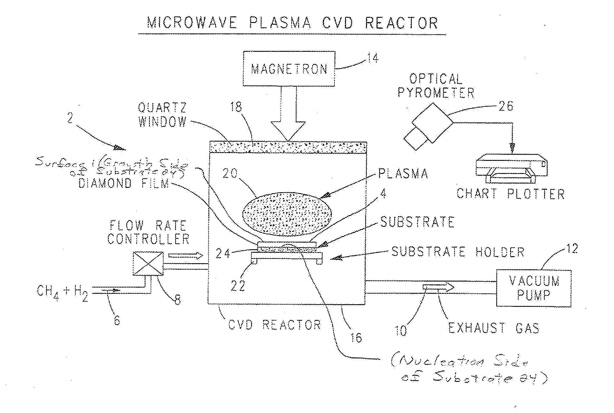
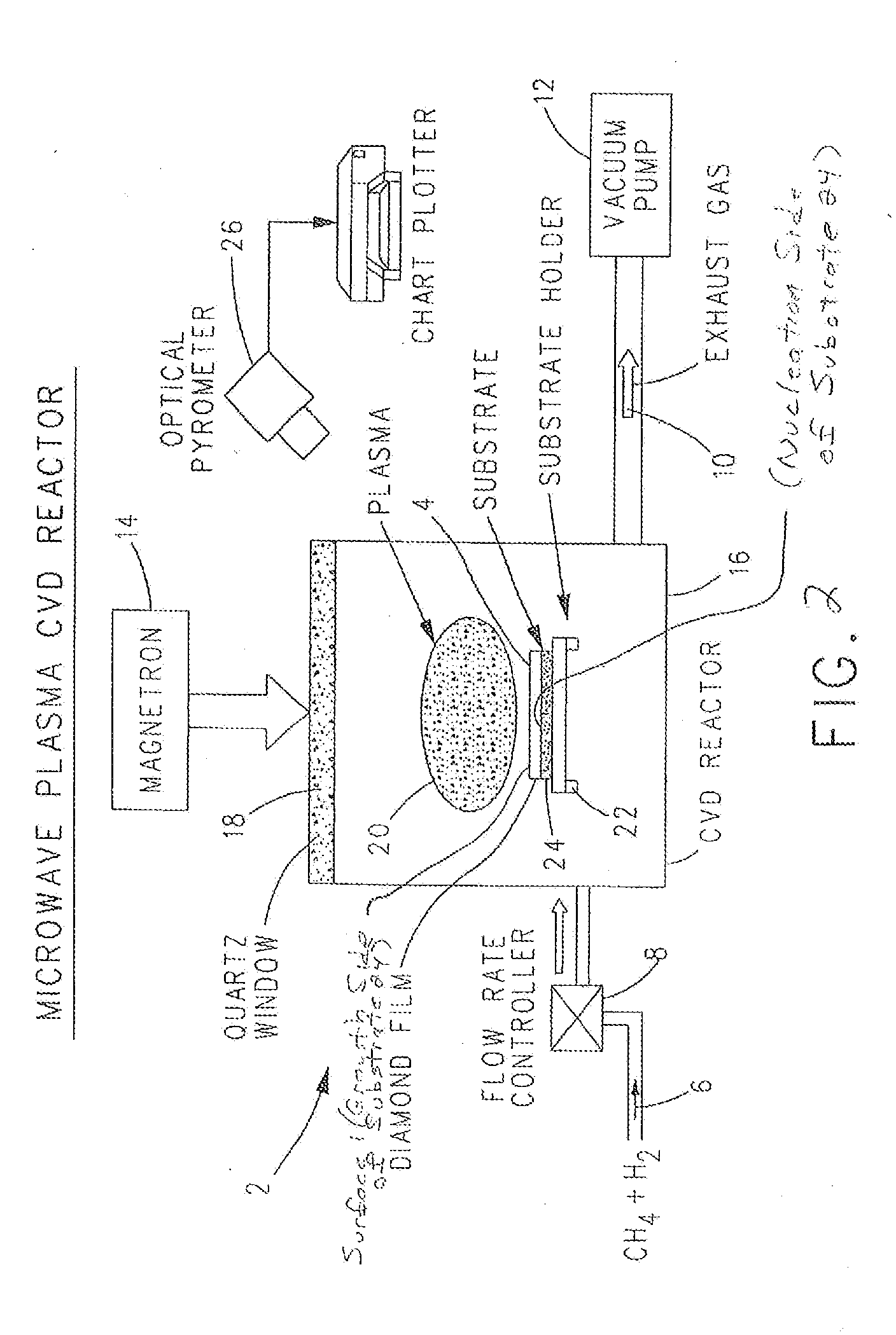
[0106]With reference to FIG. 3A-3C and with continuing reference to FIG. 2, in an example, a piece of single crystal silicon 66 mm in diameter and 11.5 mm in thickness was fabricated using a typical silicon fabrication process and used as silicon substrate 24. Surface 1 of substrate 24 was diamond-turned to an optical-finish surface with a Ra of 6 to 7 nm. A logo “II-VI” was also machined recessively by diamond-turning a “II-VI” pattern of trenches into Surface 1 of silicon substrate 24. Then, silicon substrate 24 was placed in CVD reactor 16, with the diamond-turned optically-finished surface (Surface 1) facing toward quartz window 18. A mixture of reactive gases 6 comprising hydrogen and methane, e.g., 1,850 mL / min hydrogen and 13.6 mL / min methane, was flowed into microwave plasma CVD reactor 16 under the control of mass flow controller 8. After plasma 20 ignition, magnetron 14 power and reactor 16 pressure were tune...

example 2

Producing Diamond Films with One or Two Surfaces Having an Optical Finish

[0110]In another example, a piece of single crystal silicon 2 inches (50.8 mm) inches in diameter and 10 mm in thickness was fabricated using a typical silicon fabrication process and used as silicon substrate 24. Both surfaces of this silicon substrate 24 were optically finished via a typical chemical-mechanical polishing process to an Ra of less than 1 nm. Then, this entire silicon substrate 24 was ultrasonically-treated with a diamond (0.25 microns)-ethanol suspension slurry. This silicon substrate 24 was then placed in a CVD reactor 16, with one of the optically-finished surfaces facing quartz window 18. A mixture of reactive gases 6, e.g., 1,850 mL / min hydrogen and 13.6 mL / min methane, was flowed into the microwave plasma CVD reactor 16. After plasma 20 ignition, magnetron 14 power and reactor pressure 16 were tuned so that the plasma 20 size covered the surface of silicon substrate 24 facing quartz window...

example 3

Diamond Film(s) Grown on a Single Crystal Si Substrate (166 mm Diameter×10 mm Thickness) with Both Surfaces Chemically-Etched—Producing a Diamond Film with One Surface Having an Optical Finish

[0113]In another example, a piece of single crystal silicon 166 mm in diameter and 10 mm in thickness was fabricated using a typical silicon fabrication process and used as silicon substrate 24. Both surfaces of this silicon substrate 24 were finished via typical chemical-etching process to a surface roughness (Ra) of 918 nm. Then, this entire silicon substrate 24 was rubbed with diamond powders and placed in CVD reactor 16 (FIG. 2). A mixture of reactive gases 6, e.g., 2,800 mL / min hydrogen and 84 mL / min methane, was flowed into microwave plasma CVD reactor 16 under the control of mass flow controller 8. After plasma 20 ignition, magnetron 14 power and reactor 16 pressure were tuned so that the plasma 20 size covered the surface of silicon substrate 24 facing quality window 18. The diamond gro...


PUM

PropertyMeasurementUnit
thicknessaaaaaaaaaa
thicknessaaaaaaaaaa
thicknessaaaaaaaaaa

Abstract

In a method of forming a diamond film, substrate, or window, a silicon substrate is provided and the diamond film, substrate, or window is CVD grown on a surface of the silicon substrate. The grown diamond film, substrate, or window has an aspect ratio ≧100, wherein the aspect ratio is a ratio of a largest dimension of the diamond film, substrate or window divided by a thickness of the diamond film. The silicon substrate can optionally be removed or separated from the grown diamond film, substrate, or window.

Description

CROSS REFERENCE TO RELATED APPLICATION[0001]This application claims priority to U.S. Provisional Application No. 62 / 148,339, filed Apr. 16, 2015, the contents of which are incorporated herein by reference.BACKGROUND OF THE INVENTION[0002]1. Field of the Invention[0003]The present application relates to a thin diamond film, substrate, or window that has at least one optically-finished surface. The diamond film, substrate, or window has a large aspect ratio, defined as a largest dimension over thickness. The present invention also relates to a process of producing the diamond film, substrate, or window.[0004]2. Description of Related Art[0005]Diamond is the hardest material known, having a Mohs Hardness of 10, which makes diamond useful for applications such as cutting, machining, drilling, milling, etc. Diamond is also the most thermally conductive material known, having a thermal conductivity up to 2000 to 2200 watts per meter per Kelvin, which makes it desirable for applications in...

Claims


Application Information

Patent Timeline
Patent Type & Authority Applications(United States)
IPC IPC(8): C23C16/27C23C16/511
CPCC23C16/511C23C16/274C23C16/01C23C16/02C23C16/56C23C16/0254
Inventor XU, WEN-QINGANDERSON, THOMAS E.BARBAROSSA, GIOVANNIEISSLER, ELGIN E.LIU, CHAOTANNER, CHARLES D.
Owner II VI DELAWARE INC
Why Eureka
Try Eureka