Thermally enhanced face-to-face semiconductor assembly with built-in heat spreader and method of making the same
Inactive Publication Date: 2016-12-01
BRIDGE SEMICON
View PDF3 Cites 9 Cited by
Summary
Abstract
Description
Claims
Application Information
AI Technical Summary
This helps you quickly interpret patents by identifying the three key elements:
Problems solved by technology
Method used
Benefits of technology
Benefits of technology
The present invention provides a face-to-face semiconductor assembly that reduces interconnect length between top and bottom semiconductor devices, leading to superior electrical performance. It also allows for staged fan-out routing to improve production yield and lower cost. The bottom semiconductor device is attached to a heat spreader to effectively dissipate heat and improve thermal performance of the assembly. These technical effects offer significant advantages and improvements in performance, efficiency, and reliability of the face-to-face semiconductor assembly.
Problems solved by technology
Since the bottom chip is not protected and has to be thinner than the solder ball(s) for external connection, the assembly is not reliable and cannot be used in practical applications.
Although there is no TSV in the stacked chips, the TSV in the interposer that serves for circuitry routing between chips induces complicated manufacturing processes, high yield loss and excessive cost.
Additionally, as semiconductor devices are susceptible to performance degradation at high operation temperatures, stacking chips with face-to-face configuration without proper heat dissipation would worsen devices' thermal environment and may cause immediate failure during operation.
Method used
Image
Click on the blue label to locate the original text in one second.
Reading with bidirectional positioning of images and text.
Examples
embodiment 1
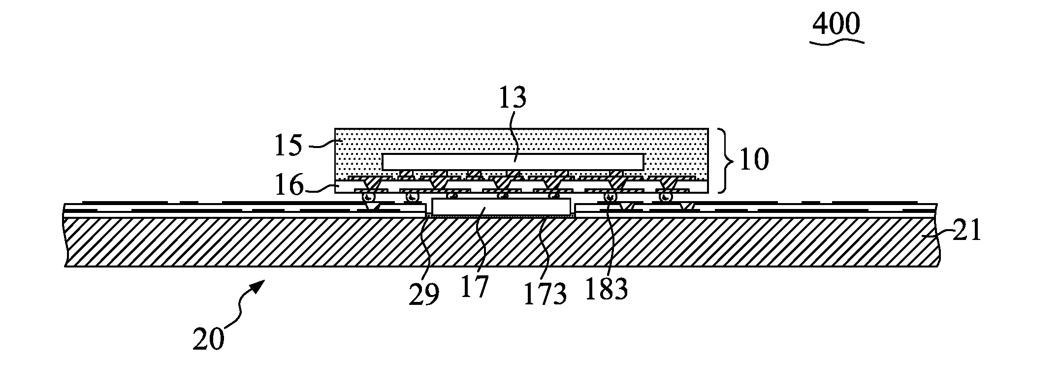
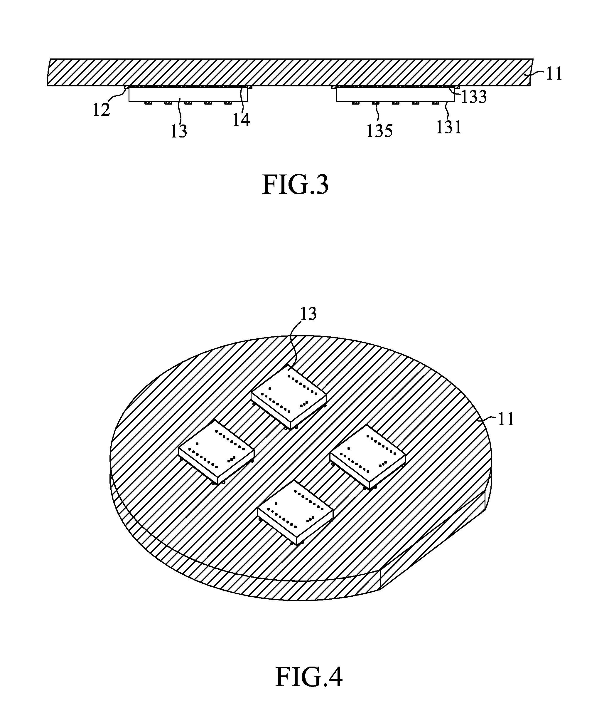
[0063]FIGS. 1-30 are schematic views showing a method of making a face-to-face semiconductor assembly that includes a stiffener 11, an alignment guide 12, a first semiconductor device 13, a balance layer 15, a first routing circuitry 16, a second semiconductor device 17, a heat spreader 21 and a second routing circuitry 24 in accordance with the first embodiment of the present invention.
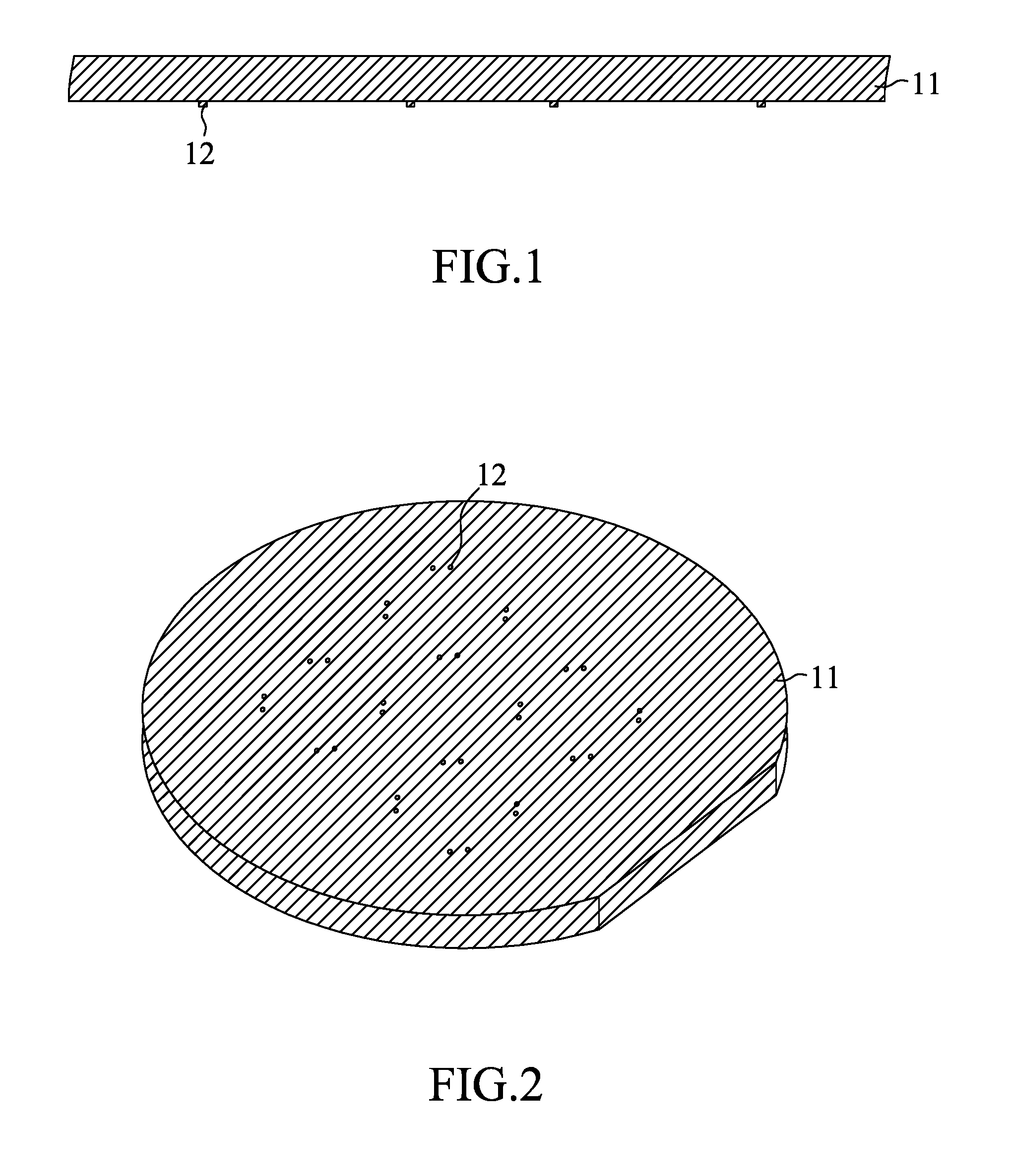
[0064]FIGS. 1 and 2 are cross-sectional and bottom perspective views, respectively, of the structure with multiple sets of alignment guides 12 on a stiffener 11. The stiffener 11 typically is made of a thermally conductive material, such as metal, alloy, silicon, ceramic or graphite, but any other thermally non-conductive material, such as mold compound, also may be used. The thickness of the stiffener 11 preferably ranges from 0.1 to 1.0 mm. The alignment guides 12 project from the bottom surface of the stiffener 11 and can have a thickness of 5 to 200 microns. In this embodiment, the stiffener 11 h...
embodiment 2
[0091]FIGS. 31-44 are schematic views showing a method of making another face-to-face semiconductor assembly that includes another aspect of subassembly in accordance with the second embodiment of the present invention.
[0092]For purposes of brevity, any description in Embodiment 1 above is incorporated herein insofar as the same is applicable, and the same description need not be repeated.
[0093]FIG. 31 is a cross-sectional view of the structure with primary conductive traces 161 formed on a sacrificial carrier 19 by metal deposition and metal patterning process. In this illustration, the sacrificial carrier 19 is a single-layer structure. The sacrificial carrier 19 typically is made of copper, aluminum, iron, nickel, tin, stainless steel, silicon, or other metals or alloys, but any other electrically conductive or non-conductive material also may be used. In this embodiment, the sacrificial carrier 19 is made of an iron-based material.
[0094]FIG. 32 is a cross-sectional view of the s...
embodiment 3
[0109]FIGS. 45-52 are schematic views showing a method of making yet another face-to-face semiconductor assembly that includes yet another aspect of subassembly in accordance with the third embodiment of the present invention.
[0110]For purposes of brevity, any description in Embodiments above is incorporated herein insofar as the same is applicable, and the same description need not be repeated.
[0111]FIG. 45 is a cross-sectional view of the structure with a first routing circuitry 16 detachably adhered over a sacrificial carrier 19. In this illustration, the sacrificial carrier 19 is a double-layer structure and includes a support sheet 191 and a barrier layer 192 deposited on the support sheet 191. The first routing circuitry 16 is the same as that illustrated in FIG. 33 and formed on the barrier layer 192. The barrier layer 192 can have a thickness of 0.001 to 0.1 mm and may be a metal layer that is inactive against chemical etching during chemical removal of the support sheet 191...
PUM
Abstract
A face-to-face semiconductorassembly is characterized in that first and second semiconductor devices are face-to-face mounted on two opposite sides of a first routing circuitry and is further electrically connected to an interconnect board through the first routing circuitry. The interconnect board has a heat spreader to provide thermal dissipation for the second semiconductor device, and a second routing circuitry formed on the heat spreader and electrically coupled to the first routing circuitry. The first routing circuitry provides primary fan-out routing for the first and second semiconductor devices, whereas the second routing circuitry provides further fan-out wiring structure for the first routing circuitry.
Description
CROSS REFERENCE TO RELATED APPLICATIONS[0001]This application claims the benefit of filing date of U.S. Provisional Application Ser. No. 62 / 166,771 filed May 27, 2015. The entirety of said Provisional Application is incorporated herein by reference.FIELD OF THE INVENTION[0002]The present invention relates to a face-to-face semiconductor assembly and, more particularly, to a face-to-face semiconductor assembly having semiconductor devices face-to-face mounted on a first routing circuitry and further electrically connected to a second routing circuitry on a heat spreader through the first routing circuitry, and a method of making the same.DESCRIPTION OF RELATED ART[0003]Market trends of multimedia devices demand for faster and slimmer designs. One of assembly approaches is to interconnect two chips with “face-to-face” configuration so that the routing distance between the two chips can be the shortest possible. As the stacked chips can talk directly to each other with reduced latency,...
Claims
Application Information
Patent Timeline
Application Date:The date an application was filed.
Publication Date:The date a patent or application was officially published.
First Publication Date:The earliest publication date of a patent with the same application number.
Issue Date:Publication date of the patent grant document.
PCT Entry Date:The Entry date of PCT National Phase.
Estimated Expiry Date:The statutory expiry date of a patent right according to the Patent Law, and it is the longest term of protection that the patent right can achieve without the termination of the patent right due to other reasons(Term extension factor has been taken into account ).
Invalid Date:Actual expiry date is based on effective date or publication date of legal transaction data of invalid patent.

