Composite structure based on ce: yag wafer, and manufacturing method thereof

a technology of composite structure and ce, applied in the field of optics, can solve the problems of weak application effect of ce and yag wafer, and achieve the effects of less machining mode, reduced cost and simple process

Inactive Publication Date: 2017-01-12
KUSN KAIWEI ELECTRONICS
View PDF9 Cites 3 Cited by
  • Summary
  • Abstract
  • Description
  • Claims
  • Application Information

AI Technical Summary

Benefits of technology

[0019]1) lower cost, more machining modes and simpler process; and
[0020]2) higher light yield, better time characteristic, wider emission spectra and better color effect.

Problems solved by technology

However, in some occasions in need of long wavelength based detection or illumination, the application of the Ce:YAG wafer has weaker effectiveness as the emission of the wafer has a main light emitting peak within the range of 525 nm-550 nm, a peak width of about 65-70 nm and relatively single wavelength.

Method used


Image

  • Composite structure based on ce: yag wafer, and manufacturing method thereof
  • Composite structure based on ce: yag wafer, and manufacturing method thereof
  • Composite structure based on ce: yag wafer, and manufacturing method thereof

Examples


embodiment 1

[0030]A Eu:Y2O3 film was coated by the sputtering method. Powdery Eu:Y2O3 was prepared first. The molar concentration of Eu ions is 0.2%. The powdery Eu:Y2O3 is then pressed into a bulk target. The Eu:Y2O3 target was attached to a cathode of a coating machine. A Ce:YAG wafer (the molar concentration of Ce ions is 0.3%) prepared by a pulling method is cut into the required size and polished. The Ce:YAG wafer was cleaned and then attached to an anode opposite to the target surface. The system was vacuumed to high vacuum (10−3 Pa) and then charged with 5 Pa argon.

[0031]Voltage was applied between the cathode and the anode to begin coating. Vacuuming operation was performed after coating, then nitrogen was charged for cold cutting, and a Ce:YAG wafer composite light emitting structure coated with a Eu:Y2O3 red light emitting film was finally obtained.

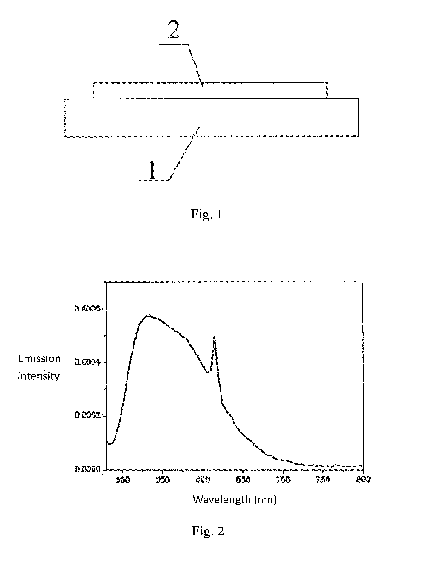
[0032]FIG. 2 is an emission spectrum of the composite structure coated with a Eu:Y2O3 film in Embodiment 1. It can be seen from the spectr...

embodiment 2

[0033]A red fluorescent powder film was coated by way of gumming 0.05 wt % of red fluorescent powder is added into silica gel. The mixture was uniformly stirred and uniformly sprayed onto the surface of a Ce:YAG wafer (the molar concentration of Ce ions is 0.3%, and the Ce:YAG wafer is prepared by a temperature gradient method). Then the Ce:YAG wafer was braked for 3 hours at 120° C. A Ce:YAG wafer composite light emitting structure coated with a red fluorescent powder film was obtained after the gel is cured.

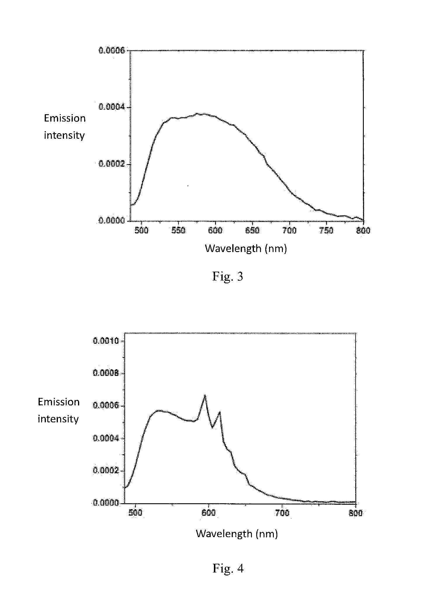
[0034]FIG. 3 is an emission spectrum of the composite structure coated by way of gumming with a red fluorescent powder film in Embodiment 2. It can be seen from the spectrum that the composite structure coated with the red fluorescent powder film has the emission spectra with the width of 500 nm-750 nm, and can realize the emission ranging from green light to red light.

embodiment 3

[0035]A Eu:YAG wafer (the molar concentration of Eu ions is 0.2%, and the Eu:YAG wafer is prepared by a kyropoulos method) was laminated with a Ce:YAG wafer (the molar concentration of Ce ions is 0.5%, and the Ce:YAG wafer is prepared by a temperature gradient method) by silica gel. The surfaces of the Ce:YAG wafer and the Eu:YAG wafer were polished, so that the wafers have good finish and planeness.

[0036]The surface of the Ce:YAG wafer was applied with silica gel and covered by the Eu:YAG wafer. The wafers were baked for 3 hours at 100° C. and then slowly cooled to room temperature to form a Ce:YAG and Eu:YAG wafer composite light emitting structure.

[0037]FIG. 4 is an emission spectrum of the composite structure laminated with the Eu:YAG wafer by silica gel in Embodiment 3. It can be seen from the spectrum that the composite structure laminated with a Eu:YAG wafer by silica gel has the emission spectra with the width of 500 nm-700 nm, and can realize the emission ranging from green...


PUM

PropertyMeasurementUnit
temperatureaaaaaaaaaa

Abstract

The invention discloses a composite structure based on a Ce:YAG wafer, comprising the Ce:YAG wafer and a red light emitting layer fixed on the Ce:YAG wafer. The invention further discloses a manufacturing method of the composite structure based on a Ce:YAG wafer, through which a composite optical structure capable of emitting light ranging from green light to red light is formed. The composite optical structure can be widely applied in the fields of detection equipment and illumination devices.

Description

FIELD OF THE INVENTION[0001]The present invention relates to the field of optics, and particularly to a composite structure based on a Ce:YAG wafer and a manufacturing method thereof.BACKGROUND OF THE INVENTION[0002]The cerium ion doped yttrium aluminum garnet (Ce:Y3Al5O12 or Ce:YAG) crystal is a novel inorganic scintillation crystal appeared in the 1980s, and has a wide application prospect in the fields of high energy physics, nuclear physics, imaging nuclear medicine, industrial online detection, illumination and the like due to the advantages of higher light output, faster time decay constant and the like. Besides the higher light output (20,000 Ph / MeV) and faster time decay (88 ns / 300 ns), the Ce:YAG scintillation crystal further has good capability of distinguishing γ rays from α particles with optical pulses, can emit 550 nm fluorescence which effectively couples with a silicon photodiode, can be excited by blue light having a wavelength within a range of 435 nm-470 nm and th...

Claims


Application Information

Patent Timeline
Patent Type & Authority Applications(United States)
IPC IPC(8): C09K11/77G01T1/202
CPCG01T1/2023C09K11/7774
Inventor CAO, DUNHUALIANG, YUESHANMA, KEJUN
Owner KUSN KAIWEI ELECTRONICS
Why Eureka
Try Eureka