TFT substrate manufacturing method and TFT substrate

a thin film transistor and manufacturing method technology, applied in the field of display technology, can solve the problems of mos device failure, deterioration of device performance, and increasing severe hot carrier injection effect, so as to improve tft reliability, reduce threshold voltage drift, and reduce the effect of threshold voltage dri

Active Publication Date: 2017-02-09
SHENZHEN CHINA STAR OPTOELECTRONICS TECH CO LTD
View PDF0 Cites 8 Cited by
  • Summary
  • Abstract
  • Description
  • Claims
  • Application Information

AI Technical Summary

Benefits of technology

[0046]The efficacy of the present invention is that the present invention provides a TFT substrate manufacturing method, which applies etching to source and drain contact zones of an active layer to have heights thereof lower than a height of a channel zone in the middle and configures the source and drain contact zones in a stepwise form so that charge carriers are affected by an electric field (Vds electric field) that is deviated in a direction away from a poly-silicon/gate insulation layer interface and the migration path thereof is caused to shift away from the poly-silicon/gate insulation layer interface thereby reducing the injection of high energy carriers into the gate insulation layer. Further, due to the formation of the steps in the drain contact zone, the peak intensity of the lateral electric field (Vds electric field) around the drain contact zone and ...

Problems solved by technology

Hot carrier effect is an important mechanism of failure of metal oxide semiconductor (MOS) devices and with the size of the MOS devices being increasingly reduced, the hot carrier injection effect becomes increasingly severe.
The hot carriers may cause breaking of energy bonds at the silicon substrate and silicon oxide gate oxide interface and generate an interface state between the silicon substrate and the silicon oxide gate oxide interface, leading to deterioration of device performance, such as threshold voltage, transconductance and linear zone/saturation zone currents, and eventually resulting in failure of the MOS device.
The failure of the MOS device generally occurs at the drain terminal first.
Conse...

Method used


Image

  • TFT substrate manufacturing method and TFT substrate
  • TFT substrate manufacturing method and TFT substrate
  • TFT substrate manufacturing method and TFT substrate

Examples


Embodiment Construction

[0058]To further expound the technical solution adopted in the present invention and the advantages thereof, a detailed description is given to a preferred embodiment of the present invention and the attached drawings.

[0059]Referring to FIGS. 1-10, firstly, the present invention provides a thin-film transistor (TFT) substrate manufacturing method, which comprises the following steps:

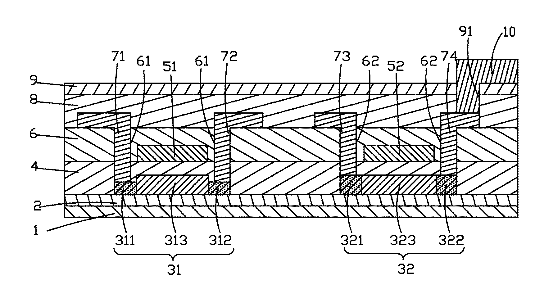
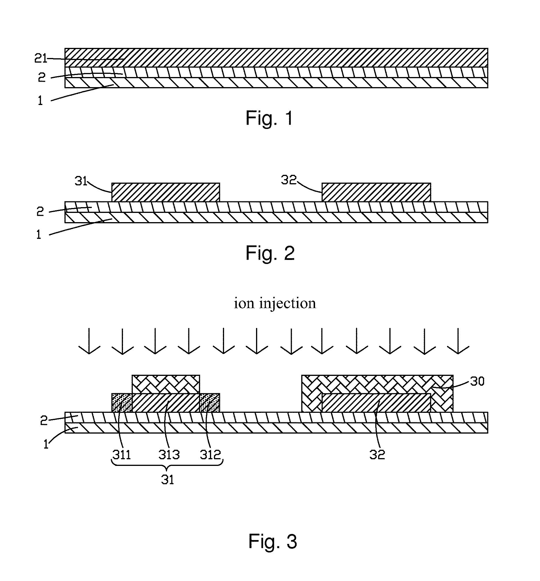
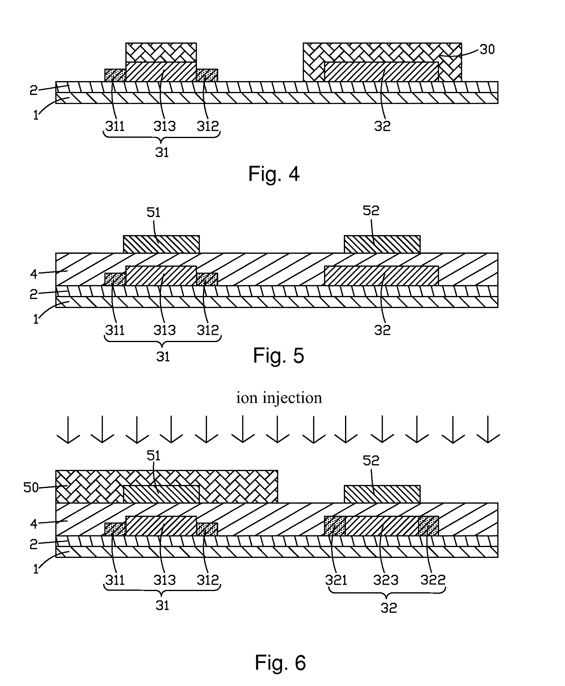
[0060]Step 1: as shown in FIG. 1, providing a substrate 1 and sequentially depositing a buffer layer 2 and an amorphous silicon layer 21 on the substrate 1.

[0061]Specifically, the buffer layer 2 can be a silicon oxide (SiOx) layer, a silicon nitride (SiNx) layer, or a stacked combination of a silicon oxide layer and a silicon nitride layer.

[0062]Step 2: as shown in FIG. 2, subjecting the amorphous silicon layer 21 to excimer laser annealing (ELA) or solid phase crystallization (SPC) to convert the amorphous silicon layer into a low temperature poly-silicon layer and applying a photolithographic process t...


PUM


Abstract

The present invention provides a TFT substrate manufacturing method and a TFT substrate. The TFT substrate manufacturing method of the present invention applies etching to source and drain contact zones of an active layer to have heights thereof lower than a height of a channel zone in the middle and configures the source and drain contact zones in a stepwise form so that charge carriers are affected by an electric field (Vds electric field) that is deviated in a direction away from a poly-silicon/gate insulation layer interface and the migration path thereof is caused to shift away from the poly-silicon/gate insulation layer interface thereby reducing the injection of high energy carriers into the gate insulation layer. Further, due to the formation of the steps in the drain contact zone, the peak intensity of the lateral electric field (Vds electric field) around the drain contact zone and the intensity of a longitudinal electric field (Vgs electric field) of the drain contact zone are both reduced, making a pinch-off point shifted toward an edge of the drain contact zone, reducing drifting of threshold voltage, and improving TFT reliability.

Description

BACKGROUND OF THE INVENTION1. Field of the Invention[0001]The present invention relates to the field of display technology, and in particular to a thin-film-transistor (TFT) substrate manufacturing method and a TFT substrate.2. The Related Arts[0002]Thin-film transistors (TFTs) are currently the primary driving device of liquid crystal displays (LCDs) and active matrix organic light-emitting diodes (AMOLEDs) and are directly related to the development of high performance flat panel display devices. The TFTs have various structures and there are various materials that are used to make the corresponding ones of the TFT structures. Low temperature poly-silicon (LTPS) material is one of the preferred materials. The regular arrangement of atoms of LTPS makes the mobility of charge carriers high. For the liquid crystal displays that are driven by voltage, due to the relatively high mobility that a poly-silicon thin-film transistor may have, driving liquid crystal molecules to rotate can b...

Claims


Application Information

Patent Timeline
IPC IPC(8): H01L29/786H01L27/12
CPCH01L29/78618H01L27/1222H01L29/78696H01L27/1288H01L29/78675H01L27/1274
Inventor LU, MACAI
Owner SHENZHEN CHINA STAR OPTOELECTRONICS TECH CO LTD
Why Eureka
Try Eureka