Chemically-sensitive field effect transistors, systems, and methods for manufacturing and using the same

a field effect transistor and chemically sensitive technology, applied in solid-state devices, material analysis, instruments, etc., can solve the problems of large volume of required instruments for performing such high-throughput sequencing, inability to carry, and large time and effort that goes into building full-length genomic sequences

Active Publication Date: 2017-04-13
CARDEA BIO INC
View PDF0 Cites 45 Cited by
  • Summary
  • Abstract
  • Description
  • Claims
  • Application Information

AI Technical Summary

Benefits of technology

[0026]One aspect of the present disclosure is a chemically-sensitive field effect transistor (FET). These chemically-sensitive FETs are preferably fabricated using semiconductor fabrication methods on a semiconductor wafer used for semiconductor manufacturing, and in preferred embodiments, on top of an integrated circuit structure made using semiconductor fabrication methods. The instant chemically-sensitive FETs typically comprise a conductive source, a conductive drain, and a channel composed of a one-dimensional (1D) or two-dimensional (2D) and/or three-dimensional (3D) transistor material, which channel extends from the source to the drain and may be fabricated using semiconductor fabrication techniques on top of a wafer. For instance, a substrate, such as a silicon substrate may be provided, upon which a non-conductive layer, e.g., an oxide layer, may be positioned, within which the source and drain electrodes may be deposited, and a channel member formed there between, which channel member may additionally be at least partially covered or coated with another non-conductive layer, such as an oxide layer. Specifically, in various embodiments, a non-conductive, e.g., oxide, layer may be disposed on the channel member and/or across the channel region. In some embodiments, chemically-sensitive FET may also include a gate or gate region, e.g., a solution gate, and/or a reference electrode. A processor and associated circuitry may also be included or otherwise be functionally associated with a chemically-sensitive FET of the disclosure (array thereof) in order to process and analyze signals generated thereby.
[0027]In use, desired chemical reactions that occur in proximity to the chemically-sensitive FET result in a change in conductance that can be sensed. Particularly, changes in conductance through the 1D, 2D, and/or 3D channel member connecting the source and the drain electrodes may be detected. For instance, in some embodiments, sensing of a desired reaction produces an alteration, e.g., a shift, in an I-V curve, for example, an I-Vg curve, or a parameter of an I-Vg curve, e.g., the curve's slope or position relative to the horizontal axis, corresponding to the chemically-sensitive field effect transistor. A processor functionally associated with the chemically-sensitive FET may be used to compare a reference I-V curve (or parameter thereof) for the well (or other capture region or structure) and an I-V curve (or the corresponding parameter thereof) generated in connection with a chemical reaction in well (or other capture region ...

Problems solved by technology

As will be appreciated, a central challenge in DNA sequencing based on the sequencing of numerous short DNA fragments is assembling full-length genomic sequences, e.g., chromosomal sequences, from a sample of genetic material, as the sequencing methods used in NGC processes do not produce full-length gene or chromosomal sequences from the sample DNA that can then be used for a desired genetic analysis, e.g., SNP genotyping, assessment of genetic variation or identity between the subject's sample and a reference gene, genome, etc.
Even so, as the human genome comprises approximately 3.1 billion base pairs, and as each sequence fragment in an NGS process is typically only from 100 to 500 to 1,000 nucleotides in length, the time and effort that goes into building full-length genomic sequences and determining the genetic variants therein is quite extensive, often requiring the use of several different computer resources applying several different algorithms over prolonged periods of time.
To provide this over-representation, increased sample preparation may be required, thus making the process more expen...

Method used


Image

  • Chemically-sensitive field effect transistors, systems, and methods for manufacturing and using the same
  • Chemically-sensitive field effect transistors, systems, and methods for manufacturing and using the same
  • Chemically-sensitive field effect transistors, systems, and methods for manufacturing and using the same

Examples


example 1

Manufacture of a 2D GFET

[0477]As shown in FIGS. 34-47, in some embodiments manufacturing a well for a 2D material FET involves an organic protective layer or an inorganic protective layer.

[0478]For a well with an inorganic protective layer, PECVD oxide, LPCVD Oxide, or Nitride LPCVD are preferred, at least for the nitride, as the film has a lower stress and less tendency to crack. Most of the well depth is created by a photoresist pattern process and RIE. The final amount of well depth can be created by a wet etch process. An alternative is to deposit a thin SiN layer, then a thick SiO2 layer. The SiO2 is patterned and etched with a highly selective etch, in a preferred embodiment, SiN acts as an ESL. Then a final wet etch process is performed on the SiN from the bottom of the well. Yet another option is to use a low temperature TEOS oxide, which is a denser, less porous oxide. It prevents uptake of contaminants or reaction materials in the oxide that may affect results.

[0479]For or...

example 2

Manufacture of a 2D GFET

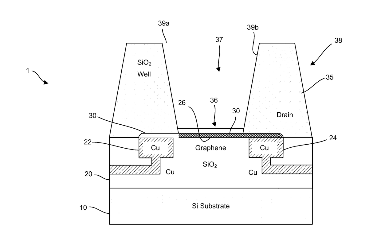
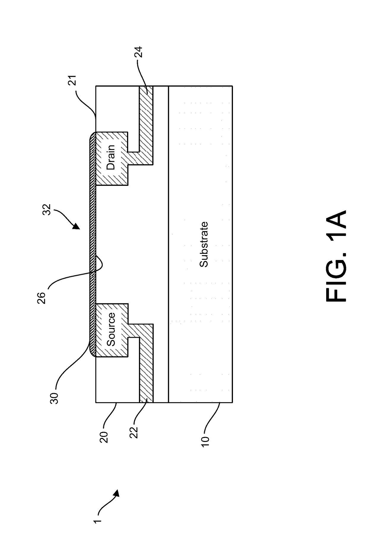
[0503]A preferred representative method for manufacturing a FET for chemical and biological analysis is shown in FIGS. 48-51. The method includes depositing a graphene channel on an exposed metal layer of an integrated circuit structure. The integrated circuit structure comprises a semiconductor substrate, a dielectric layer, and the metal layer. The method also includes utilizing a patterned material to expose a portion of a channel area and a plurality of adjacent areas. The method also includes etching the dielectric material starting with the adjacent areas thereby exposing a trench under the channel and exposing the metal in the channel area. The method also includes etching the metal from underneath the graphene channel to create a chemically-sensitive FET.

[0504]This method uses a full CMOS wafer with top copper electrodes exposed by CMP. In this case there is also copper in the channel area (512). A graphene layer (26) is deposited (e.g., via PECVD or ...

example 3

Manufacture of a Growth Substrate

[0520]FIG. 17 shows a flow chart of a general method of forming a semiconductor wafer with transistors having 2D material layers. FIGS. 25A-25F illustrate the various steps.

[0521]A preferred direct transfer mechanism, direct transfer fusion bonding, is shown in FIGS. 25A-25F. FIGS. 25A-25F visually show the steps of direct bond transfer via fusion bonding. In FIG. 25A, the 2D material (521), preferably graphene, is grown on a growth platform (520) composed of a platinum layer (522) on a growth wafer (523). In FIG. 2B, a cover material (524) and CMP or polish surface is deposited on the growth platform (523). In FIG. 25C, the growth platform (520) is flipped. In FIG. 25D, a ROIC wafer (525) is prepared, and the ROIC wafer (525) and the growth platform (520) are then aligned for bonding. In FIG. 25E, the cover material (524) is bonded to the ROIC wafer top insulator layer (526). In FIG. 25F, the growth substrate (527) is separated from the ROIC wafer, ...


PUM


Abstract

This invention concerns chemically-sensitive field effect transistors (FETs) are preferably fabricated using semiconductor fabrication methods on a semiconductor wafer, and in preferred embodiments, on top of an integrated circuit structure made using semiconductor fabrication methods. The instant chemically-sensitive FETs typically comprise a conductive source, a conductive drain, and a channel composed of a one-dimensional (1D) or two-dimensional (2D) transistor material, which channel extends from the source to the drain and is fabricated using semiconductor fabrication techniques on top of a wafer. Such chemically-sensitive FETs, preferably configured in independently addressable arrays, may be employed to detect a presence and/or concentration changes of various analyte types in chemical and/or biological samples, including nucleic acid hybridization and/or sequencing reactions.

Description

CROSS REFERENCE TO RELATED APPLICATIONS[0001]This application claims the benefit of priority to U.S. Provisional Application Ser. No. 62 / 206,228, filed on Aug. 17, 2015; U.S. Provisional Application Ser. No. 62 / 206,224, filed on Aug. 17, 2015; U.S. Provisional Application Ser. No. 62 / 205,803, filed on Aug. 17, 2015; U.S. Provisional Application Ser. No. 62 / 205,808, filed on Aug. 17, 2015; U.S. Provisional Application Ser. No. 62 / 206,166, filed on Aug. 17, 2015; U.S. Provisional Application Ser. No. 62 / 206,372, filed on Aug. 18, 2015; U.S. Provisional Application Ser. No. 62 / 206,814, filed on Aug. 18, 2015. This application is a continuation in part of U.S. application Ser. No. 15 / 225,764, filed on Aug. 1, 2016, which in turn claims benefit of U.S. Provisional Application Ser. No. 62 / 199,956, filed on Jul. 31, 2015 and U.S. Provisional Application Ser. No. 62 / 199,987, filed on Aug. 1, 2015. This application is a continuation in part of U.S. application Ser. No. 15 / 065,744, filed on M...

Claims


Application Information

Patent Timeline
IPC IPC(8): G01N27/414H01L29/417G01N27/327H01L29/16
CPCG01N27/4148H01L29/1606H01L29/4175H01L29/78603G01N27/3276H01L29/78684H01L29/41733H01L29/66409H01L21/76883H01L27/085H01L21/76879
Inventor HOFFMAN, PAUL
Owner CARDEA BIO INC
Why Eureka
Try Eureka