Integrated vertical sharp transistor and fabrication method thereof

a vertical sharp transistor and integrated technology, applied in the direction of semiconductor devices, electrical apparatus, nanotechnology, etc., can solve the problems of affecting the performance of the device, the impact of various parasitic effects became critical, and the finfet technology does not allow the implementation of bipolar transistors in one chip, so as to achieve a high dopant level

Inactive Publication Date: 2017-06-08
LESENCO DUMITRU NICOLAE
View PDF5 Cites 10 Cited by
  • Summary
  • Abstract
  • Description
  • Claims
  • Application Information

AI Technical Summary

Problems solved by technology

The size of its devices should be small accordingly, but the impact of various parasitic effects became critical.
However, FinFET technology does not allow implementation of bipolar transistors in one chip, like BiCMOS in 65 nm. technology.
The benefits in chip scalability are minimal, but compromise between low voltage / high speed operation and low power dissipation / noise interference is big problem.
The influence of parasitic effects, such as cross talk, electro migration, voltage drop, gate noise is essential problem.
Also floor plan, power supply, matching, layout design, physical design verification, DFM became very complicate in special for System on the Chip (SoC).
The FinFET technology, CAD tools, PDK and layout design for 20, 16, 14, 10, 6 nm nodes are very expensive.
The FinFET chips are not so good for space applications, because the probability of radiation impact is high.
However, this technology does not allow implementation of bipolar transistors in one chip too, and is expected to be more expensive than FinFET technology.

Method used


Image

  • Integrated vertical sharp transistor and fabrication method thereof
  • Integrated vertical sharp transistor and fabrication method thereof
  • Integrated vertical sharp transistor and fabrication method thereof

Examples


Embodiment Construction

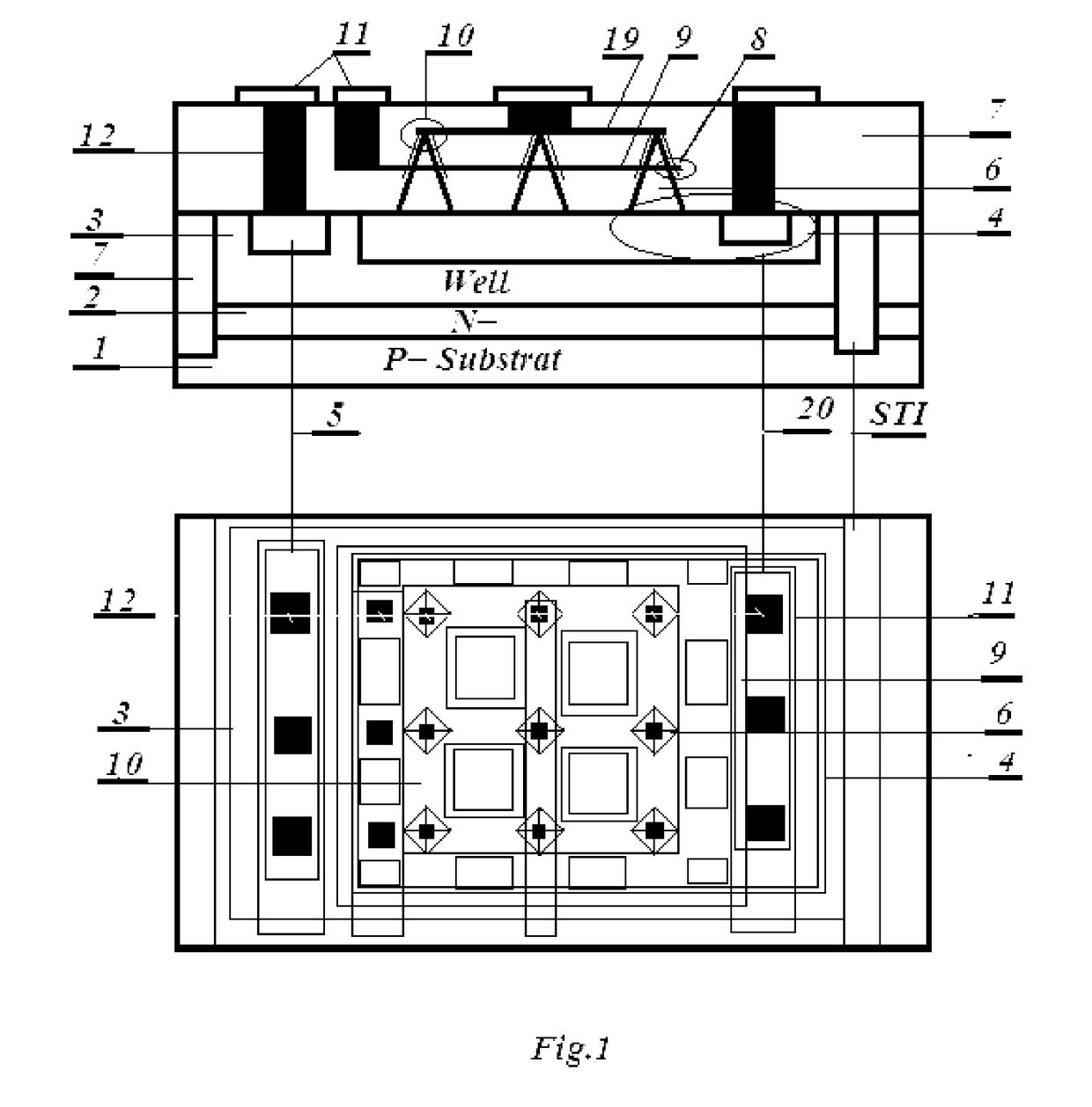
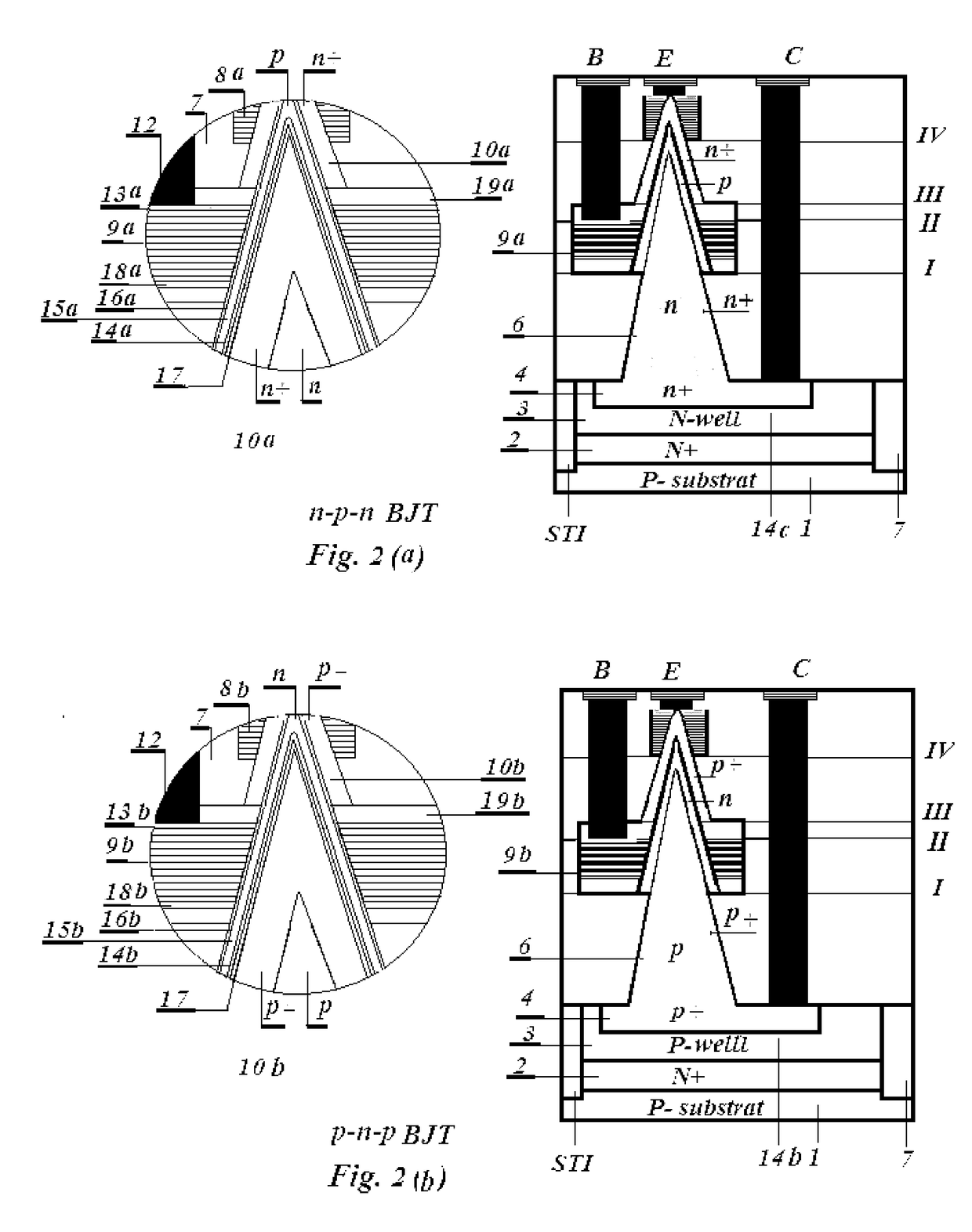
[0043]The embodiments herein will be better understood from the following detailed description that references the drawings, which are not necessarily drawn to scale. In the description of the invention, “n”, “n+”, “N”, “N+” and “p”, “p+”, “P”, and “P+” are used to define relative dopant types and concentrations. FET is used interchangeably with “field-effect transistor”, or “metal-oxide transistor”. BJT is used interchangeably with “bipolar junction transistor” or “bipolar heterojunction transistor”. COR is used interchangeably with “Composite Object Reference structure”. CMP is used interchangeable with “Chemical-Mechanical Polishing / Planarization”. RIE is used interchangeable with “Reactive Ion Etching”.

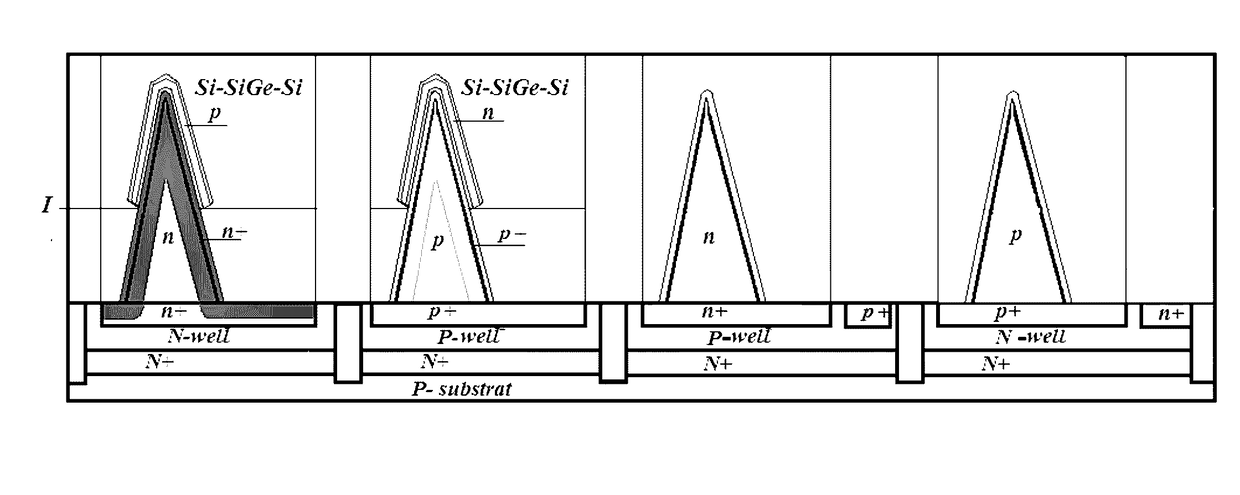
[0044]In reference to the drawings, FIG. 1. shows the general concept of the present invention. A cross section diagram and planar view illustrate a first preferred embodiment of a vertical quantized transistor such as a BJT and FET with a sharp emitter or drain fabricated, utiliz...


PUM


Abstract

The present invention relates to vertical integrated, quantized FET with sharp drain and BJT with sharp emitter implemented in one nano-BiCMOS process, using multiple identical single crystalline semiconductor pyramids, placed in-situ directly on the surface of diffusion regions. The devices' gate and base structures are formed at a level of 35-45 nm below the top of the pyramids. The bottom region of the pyramids contains the collector / source structures, while the top region of the pyramids contains the emitter / drain structures. The base structure for BJT is formed by selective epitaxial growth of Si—SixGe1-x—Si with opposite conductivity type as COR, and interconnected by a horizontal polysilicon grid. The self-aligned gate structure for FET is formed by high dopant implantation of impurity with the same type of conductivity as COR through horizontal gate bridge, which represent a grid of horizontal stacked layers Si3N4 —high-k insulator—polysilicon—high-k insulator—Si3N4.

Description

REFERENCE CITEDPatent Citations[0001][1]. U.S. Pat. No. 6,885,055 B2 Double-gate FinFET device and fabricating method thereof Apr. 26, 2005 Jong-Ho Lee . . . 257 / 618.[0002][2]. U.S. Pat. No. 7,736,979 B2 Method of forming nanotube vertical field effect transistor, Jun. 15, 2010, Reginald Conway Farrow et al.[0003][3]. U.S. Pat. No. 7,625,792 B2 Method of base formation in a BiCMOS process, Dec. 1, 2009, Peter J. Geiss et al.[0004][4]. U.S. Pat. No. 4,96,0726 BI CMOS Process, Oct. 2, 1990, John S. Leachaton et al. U.S.Cl. 437 / 59.[0005][5]. U.S. Pat. No. 7,384,835 B2 MOSFET with a sharp halo and a method of forming the transistor, Jun. 10, 2008. Haujie Chen et al U.S.Cl. 438 / 197.[0006][6]. U.S. Pat. No. 7,625,792 B2 Method of base formation in a BICMOS process, Dec. 1, 2009. Peter J. Geiss et al U.S.Cl. 438 / 202[0007][7]. U.S. Pat. No. 6,774,000 B2 Method of manufacturing of MOSFET device with in-situ doped, raised source and drain structures, Aug. 10, 2004, Wesley C. Natzle et al. U.S...

Claims


Application Information

Patent Timeline
Patent Type & Authority Applications(United States)
IPC IPC(8): H01L27/06H01L29/16H01L29/06H01L21/8249H01L29/423H01L29/10H01L21/8238H01L27/092H01L29/78H01L29/08
CPCH01L27/0623H01L29/7827H01L29/16H01L29/0657H01L29/0692H01L29/0847H01L21/8249H01L29/0804H01L29/0821H01L29/1004H01L21/823885H01L27/092H01L29/42376B82Y10/00B82Y40/00H01L29/732H01L29/735H01L29/775H01L29/0665H01L29/0676H01L29/0808H01L29/1008H01L29/155H01L29/42356
Inventor LESENCO, DUMITRU NICOLAE
Owner LESENCO DUMITRU NICOLAE
Why Eureka
Try Eureka