Methods of growing heteroepitaxial single crystal or large grained semiconductor films and devices thereon

Active Publication Date: 2017-06-29
SOLAR TECTIC
View PDF4 Cites 0 Cited by
  • Summary
  • Abstract
  • Description
  • Claims
  • Application Information

AI Technical Summary

Benefits of technology

[0028]In order to take full advantage of the invention disclosed here the semiconductor material has to be deposited on a substrate material which is inexpensive, and the surface of which enables heterogeneous nucleation and growth. In the following we shall discuss two specific methods for producing substrates suitable for heterogeneous deposition of films for photovoltaic technology. Both of these methods have been described in the scientific literature and we do not claim to invent them. We include them here for completeness.
[0029]The use of rolled and textured Ni and Ni-alloy sheets has been proposed as substrate material for superconducting films and, more recently, for films for photovoltaic devices (Findikoglu et al). In order to facilitate the growth of epitaxial superconducting films on such substrates, there have been two approaches described in the scientific literature: in one the sharp rolling texture produced in a rolled and annealed Ni alloy is used as a template on which various epitaxial buffer layers are deposited followed finally by an epitaxial film of a high temperature cuprate superconductors (Goyal et al). In the second approach (Findikoglu et al), the nickel ribbon is used as a substrate for ion beam assisted deposition of a wide variety of highly textured ceramics, for example, magnesium oxide (MgO). The ion beam aligns the growing MgO film, which provides a template for the subsequent deposition of the cuprate superconductor.
[0030]The latter approach is not limited to using metal tapes but can be extended to other inexpensive substrates such as glass (Teplin et al). It has been found th

Problems solved by technology

A dominant factor in favor of the continual use of fossil fuels is their cost per unit of available energy.
A major cost component in photovoltaic cells is the cost of the substrate on which the semiconductor film capable of converting sunlight into electricity is placed.
If a silicon film could be deposited on an inexpensive substrate, such as glass, and with comparable quality as that found in silicon single crystals used in the microelectronics industry, the cost of photovoltaic technology would drop significantly.
In contrast to metals, semiconductors, such as silicon, are difficult to grow epitaxially.
A disadvantage in this approac

Method used


Image

  • Methods of growing heteroepitaxial single crystal or large grained semiconductor films and devices thereon
  • Methods of growing heteroepitaxial single crystal or large grained semiconductor films and devices thereon
  • Methods of growing heteroepitaxial single crystal or large grained semiconductor films and devices thereon

Examples


example 1

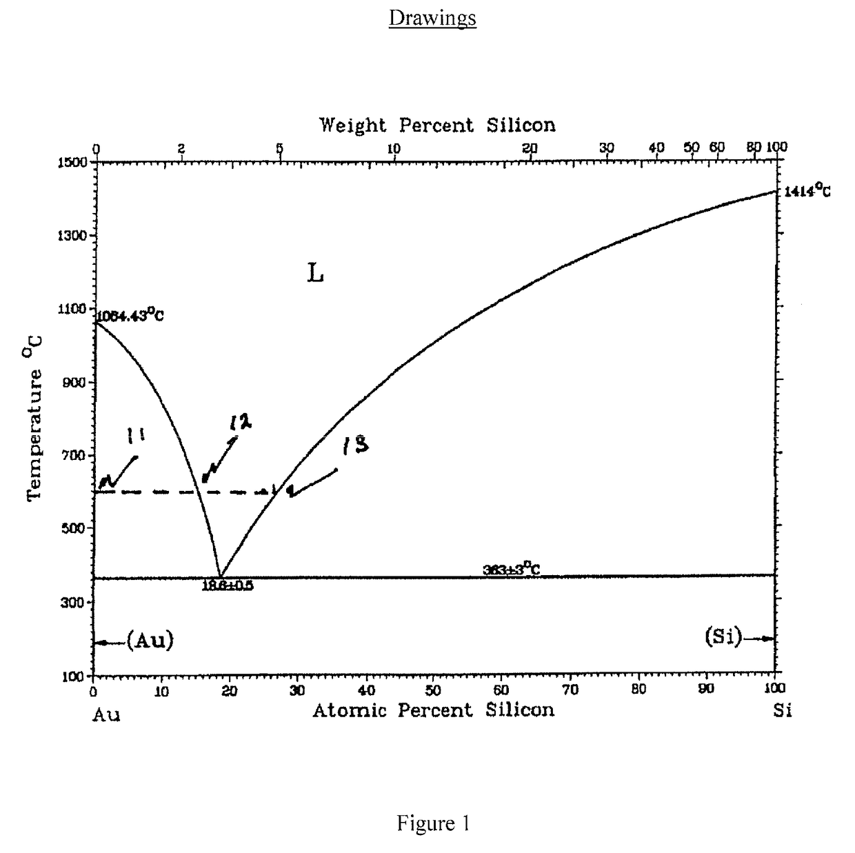
[0061]A good high vacuum system with two electron beam guns, is used to deposit gold and silicon independently. A glass substrate coated with ion beam assisted deposited MgO film is held at temperatures between 575 and 600° C. These are nominal temperatures. It is understood to one skilled in the art that lower or higher temperatures can also be used depending upon the softening temperature of the glass substrate or the reaction kinetics of either gold or silicon with the metallic tape or its buffer layers when used as substrates. A thin gold film of approximately 10 nm thickness is deposited first. This is followed by a silicon film deposited at a rate of 2 nm per minute on top of the gold film. The ratio of the thickness of the gold and silicon films is chosen such that the final composition ensures that a point, marked 13, in FIG. 1 is reached. This point lies at the boundary between the two phase region of solid Si and a liquid Si—Au mixture. For example, for a 10 nm gold film f...

example 2

[0066]A good high vacuum system with two electron beam guns is used to deposit aluminum and silicon independently. A glass substrate or a Ni based substrate coated with a buffer layer of Al2O3 is held at temperatures between 600 and 615 degree ° C. These are nominal temperatures. It is understood to one skilled in the art that lower or higher temperatures can also be used depending upon the softening temperature of the glass substrate or the reaction kinetics of either aluminum or silicon with the metallic tape or its buffer layers when used a substrates. The eutectic Al—Si is used instead of the Au—Si example above. A thin Al film 6 nm thick is deposited on the Al2O3 followed by a 100 nm thick silicon deposition, and as described in example 1, above, the two phase region comprising of solid silicon and a liquid Si—Al mixture is reached. The deposition is stopped and the sample is slowly cooled to room temperature. Aluminum diffuses through the silicon film, driven by its lower surf...

example 3

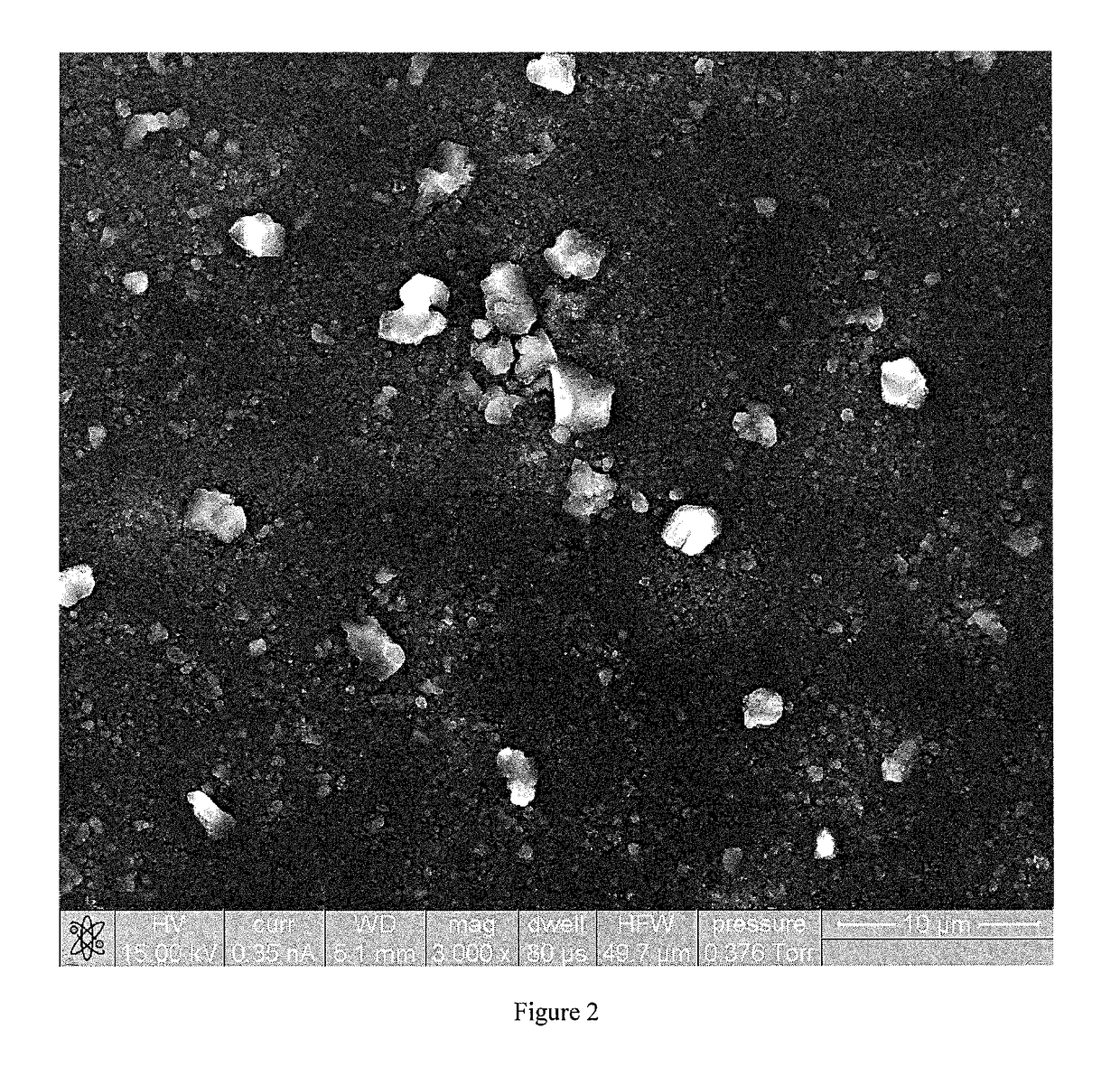
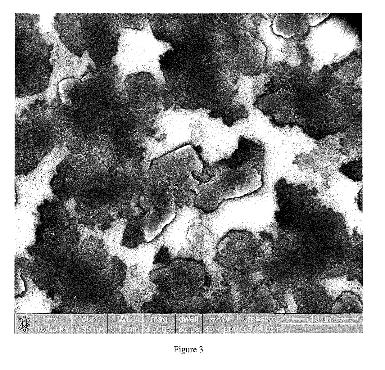
[0068]We describe in this example how different methods of deposition can be combined to take advantage of highly textured films as described in example 1, above. The Si film produced from the deposition of example 1 is etched to remove the Au and then placed back into the vacuum chamber and p+-Si is deposited on this film. This latter layer serves two purposes: it provides a conducting layer for a photovoltaic device to be subsequently built on it and can be the starting point for a variety of differently configured photovoltaic devices as, for example, a nanowire photovoltaic device. Here a 2-3 nm thick gold film is deposited on the silicon using an electron gun. This 2-3 nm thick gold film breaks up into nanoparticles and is the starting point used by a number of investigators to use chemical vapor deposition to grow nanowires and use these nanowires for photovoltaic devices. The difference is that we show how an inexpensive buffered glass can be used rather than a relatively exp...


PUM


Abstract

A method is provided for making smooth crystalline semiconductor thin-films and hole and electron transport films for solar cells and other electronic devices. Such semiconductor films have an average roughness of 3.4 nm thus allowing for effective deposition of additional semiconductor film layers such as perovskites for tandem solar cell structures which require extremely smooth surfaces for high quality device fabrication.

Description

[0001]The present invention is a Continuation-in-Part of U.S. patent application Ser. No. 14 / 979,285, filed Dec. 22, 2015, which is a Continuation-in-Part of U.S. patent application Ser. No. 14 / 724,066, filed May 28, 2015, which is a Continuation-in-Part of U.S. patent application Ser. No. 14 / 224,675 filed Mar. 25, 2014, which is a continuation of U.S. patent application Ser. No. 13 / 929,085 filed Jun. 27, 2013, which is a continuation of U.S. patent application Ser. No. 12 / 903,750 filed Oct. 13, 2010, which is a continuation-in-part of U.S. patent application Ser. No. 12 / 774,465 filed May 5, 2010, which is a continuation of U.S. patent application Ser. No. 12 / 154,802 filed May 28, 2008, all of which are hereby incorporated by reference in their entirety.REFERENCES CITEDU.S. Patent Documents[0002]U.S. Pat. No. 4,717,688 January 1987 Jaentsch . . . 148 / 171[0003]U.S. Pat. No. 5,326,719 July 1994 Green et al. . . . 427 / 74[0004]U.S. Pat. No. 5,544,616 August 1996 Ciszek et al. . . . 117 / ...

Claims


Application Information

Patent Timeline
IPC IPC(8): H01L31/0236H01L33/22H01L33/40H01L33/24C30B29/52H01L31/18H01L33/00H01G9/20C30B23/06C30B23/02H01L31/0224H01L31/0687
CPCH01L31/02363H01L31/022425H01L33/22H01L33/40H01L33/24H01L31/0687H01L2933/0016H01L33/0054H01G9/2009C30B23/066C30B23/025C30B29/52H01L31/1804C30B19/00C30B25/02C30B25/183H01L21/0242H01L21/02422H01L21/02488H01L21/02491H01L21/02532H01L21/02603H01L21/0262H01L21/02645H01L21/02653H01L31/1836H01L31/1852Y02E10/542Y02E10/544Y02E10/547Y02P70/50
Inventor CHAUDHARI, PRAVEENCHAUDHARI, ASHOK
Owner SOLAR TECTIC
Why Eureka
Try Eureka