
Photoelectric conversion element having quantum structure using indirect transition conductor material

a photoelectric conversion element and transition conductor technology, applied in the field of photoelectric conversion elements, can solve the problems of low efficiency of two-step light absorption through quantum levels, low efficiency, and the problem of increasing sensitivity of quantum dot photosensors, etc., and achieve the effect of improving the efficiency of photoelectric conversion, sluggish improvement of photoelectric conversion efficiency, and low efficiency of two-step light absorption

Inactive Publication Date: 2017-07-13
SHARP KK +1
View PDF4 Cites 9 Cited by
  • Summary
  • Abstract
  • Description
  • Claims
  • Application Information

AI Technical Summary

Benefits of technology

The patent aims to enhance the efficiency of a photoelectric conversion element.

Problems solved by technology

One conceivable cause for this is the low efficiency of two-step light absorption through a quantum level (including a superlattice miniband or an intermediate band).
In particular, there become problems that a spectrum of absorption from the quantum level to the conduction band, which corresponds to light absorption in the second step in the two-step light absorption, has low matching with a solar light spectrum (because of the weak quantum confinement effect), and that the carriers exited to the conduction band are relaxed to the quantum level and recombined (because of the low efficiency of carrier extraction).
A quantum dot photosensor also has a problem of increasing the sensitivity resulting from the weak quantum enhancement effect and the low efficiency of carrier extraction.

Method used


Image

  • Photoelectric conversion element having quantum structure using indirect transition conductor material
  • Photoelectric conversion element having quantum structure using indirect transition conductor material
  • Photoelectric conversion element having quantum structure using indirect transition conductor material

Examples


embodiment

[0022]An embodiment of the present disclosure is described in detail below with reference to the drawings. The same portion or corresponding portions are denoted by the same reference numeral, and description thereof is not repeated. In order to make the description easy to understand, the drawings referred to below each show a simplified or illustrated configuration, or some of the constituent members are omitted. Also, the dimensional ratio between the constituent members shown in each of the drawings is not necessarily an actual dimensional ratio.

[0023]The terms used in the specification are briefly described here. However, the terms are described with respect to a configuration of the embodiment, and the present disclosure is not limited to the description of the terms.

[0024]The term “quantum layer” represents a quantum dot layer, a quantum nanowire layer, a quantum well layer, or the like, which includes a semiconductor material having a narrower bandgap than that of the semico...

experimental example 1

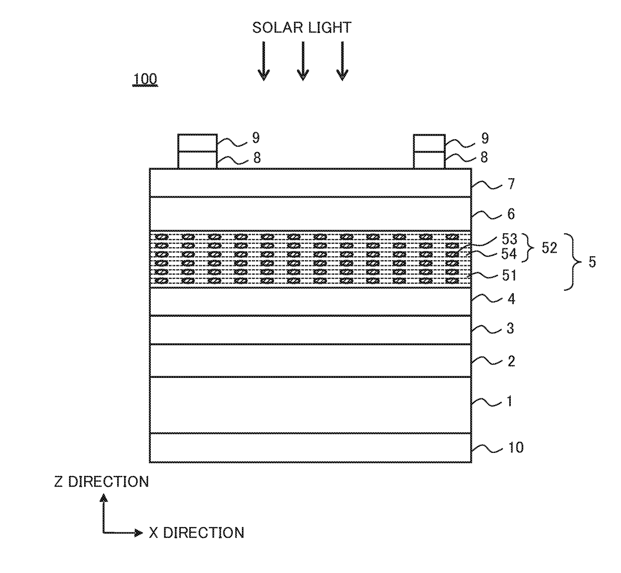
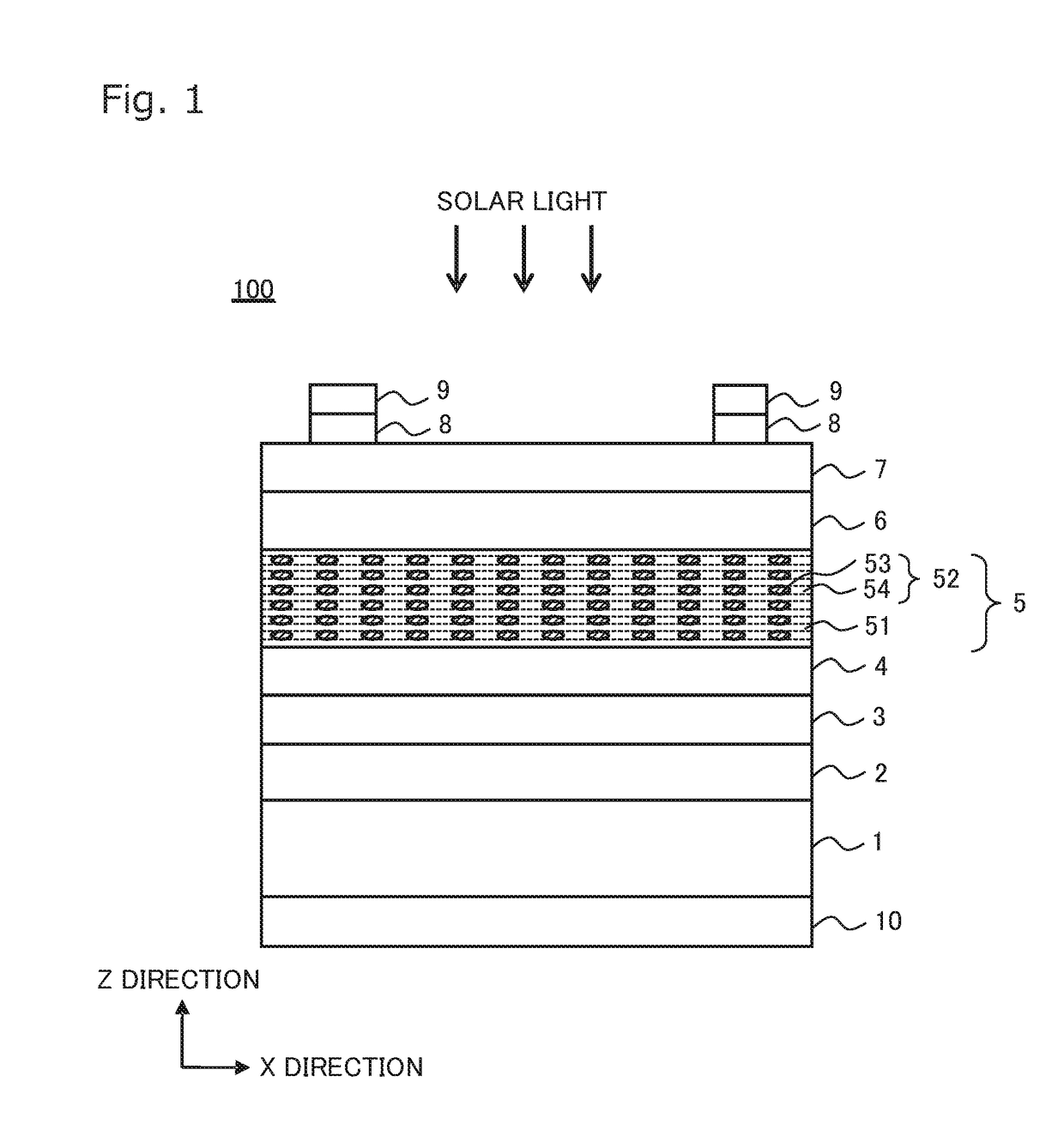
[0085]In a superlattice semiconductor layer 5 of Experimental Example 1, aluminum gallium arsenide (Al0.8Ga0.2As) was used as a base semiconductor material constituting a barrier layer 51, and indium arsenide (InAs) was used as a material of quantum dots 53. Al0.8Ga0.2As is an indirect transition semiconductor material having a bandgap at room temperature of 2.54 eV at a Γ point and 2.10 eV at an X point. That is, the bandgap at room temperature is more than 1.42 eV. InAs is a direct transition semiconductor having a bandgap at room temperature of 0.35 eV at a Γ point.

[0086]In the experimental example, AlGaAs was used as the base semiconductor material of the barrier layer 51, and InAs was used as a material of the quantum dots 53a. However, mixed crystal materials such as AlInGaAs, InGaAs, and the like, materials having different compositions, different semiconductor materials, or the like may be used.

[0087]The shape of the quantum dots 53 was a lens shape containing a wetting laye...

experimental example 2

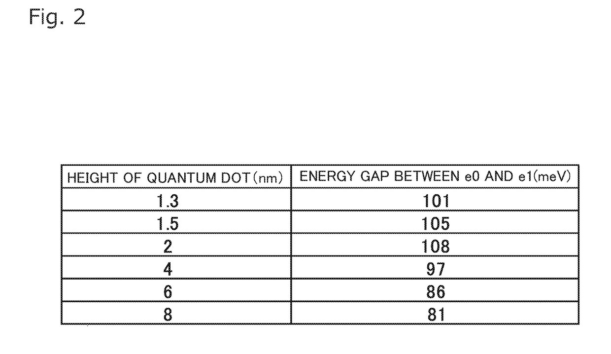
[0096]In Experimental Example 2, the same simulation experiment as in Experimental Example 1 was performed except that in the superlattice semiconductor layer 5 used in Experimental Example 1, the size (height) of the quantum dots 53 in the stacking direction was 1.3 nm, and the distance between the quantum dots 53 in the stacking direction was 4 nm.

[0097]In a configuration of a superlattice semiconductor layer 5, aluminum gallium arsenide (Al0.8Ga0.2As) was used as a base semiconductor material constituting a barrier layer 51, and indium arsenide (InAs) was used as a material of quantum dots 53. Al0.8Ga0.2As is an indirect transition semiconductor material having a bandgap at room temperature of 2.54 eV at a Γ point and 2.10 eV at an X point. That is, the bandgap at room temperature is more than 1.42 eV. InAs is a direct transition semiconductor having a bandgap at room temperature of 0.35 eV at a Γ point.

[0098]In Experimental Example 2, AlGaAs was used as the base semiconductor ma...


PUM


Abstract

A photoelectric conversion element includes a photoelectric conversion layer having the quantum structure and utilizes intersubband transition in a conduction band. The photoelectric conversion element includes a superlattice semiconductor layer in which a barrier layer and a quantum dot layer as a quantum layer are alternately and repeatedly stacked. The barrier layer includes an indirect transition semiconductor material, and the quantum dot layer has a nano-structure including a direct transition semiconductor material. The indirect transition semiconductor material constituting the barrier layer has a bandgap of more than 1.42 eV at room temperature.

Description

BACKGROUND[0001]1. Field[0002]The present disclosure relates to a photoelectric conversion element.[0003]2. Description of the Related Art[0004]Examples of a Photoelectric conversion element provided with a photoelectric conversion layer include a solar cell and a photosensor (photodetector). Various researches and developments of solar cells are carried out for the purpose of increasing the photoelectric conversion efficiency by using light within a wider wavelength region. For example, there is proposed a solar cell in which electrons are photo-excited in two steps through a quantum level (including a superlattice miniband or an intermediate band) formed between the valence band and the conduction band of a matrix material, and thus light at a long wavelength can be utilized (refer to Japanese Unexamined Patent Application Publication (Translation of PCT Application) No. 2010-509772 and PHYSICAL REVIEW LETTERS, vol. 97, p. 247701, 2006).[0005]Such a solar cell having quantum dots ...

Claims


Application Information

Patent Timeline
IPC IPC(8): H01L31/0352H01L31/109H01L31/0735H01L31/0304
CPCH01L31/035236H01L31/03046H01L31/0735H01L31/109H01L31/035218Y02E10/544H01L31/077H01L31/105Y02E10/547Y02E10/548
Inventor YOSHIKAWA, HIROFUMIIZUMI, MAKOTOARAKAWA, YASUHIKOWATANABE, KATSUYUKI
Owner SHARP KK
Learn More