Ultraviolet light emitting diodes

a light-emitting diode and ultra-violet technology, applied in the direction of basic electric elements, electrical apparatus, semiconductor devices, etc., can solve the problems of low iqe, poor eqe of deep ultra-violet leds, and high concentration of threading defects, so as to increase the extraction of light out of the device, reduce the absorption loss of the substrate, and increase the ee

Active Publication Date: 2017-07-13
TRUSTEES OF BOSTON UNIV
View PDF6 Cites 25 Cited by
  • Summary
  • Abstract
  • Description
  • Claims
  • Application Information

AI Technical Summary

Benefits of technology

[0027]In accordance with some embodiments of the invention, the surface of the n-AlGaN layer can be patterned or randomly textured to increase the extraction of light out of the device, thus increasing the EE. In accordance with some embodiments of the invention, a conductive UV AlGaN distributed Bragg reflectors (DBRs) can be disposed between the substrate (i.e., base layer) and the active region of the device to reduce absorption losses in the substrate, thus increasing the EE. In combination these two factors can lead to EE of 70-80%.
[0028]Thus, the UV LEDs of the invention can have EQE of 20-30% or more. In some applications, UV LEDs with high EQE are desirable. Some embodiments of the UV LEDs of

Problems solved by technology

Thus, the poor EQE of deep UV-LEDs may be the result of poor IQE, IE, EE or a combination of all three factors.
Due to the high lattice mismatch between AlGaN and sapphire (˜14%), such devices suffer from high concentrations of threading defects, which lower their IQE [16].
Besides the high concentration of the threading defects, another source leading to poor IQE is the incorporation of oxygen in AlGaN.
The IE of UV LEDs is limited by the relatively poor doping efficiency of the p-AlGaN (low hole density) and the low diffusion length of the injected holes.
In addition to the aforementioned absorption losses in the p-side, the EE in current UV

Method used


Image

  • Ultraviolet light emitting diodes
  • Ultraviolet light emitting diodes
  • Ultraviolet light emitting diodes

Examples


example 1

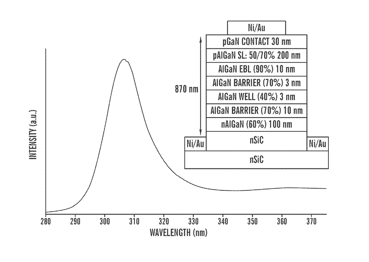
[0147]As a non-limiting example, an LED as described above can be grown on a p-SiC substrate as shown schematically in FIGS. 15A-15B. For said example, a Veeco GEN-II plasma assisted MBE system was used to grow the full device. The substrate was cleaned in situ by sequential cycles of Ga accumulation and evaporation. An undoped 40 nm thick AlN electron-blocking layer was grown using In as a surfactant. The active region consisted of 15 quantum wells 2 nm thick of 40% AlN mole fraction AlGaN alloy. Barriers for the wells consisted of 2 nm of 60% AlN mole fraction AlGaN alloy. The growth of the active region commenced with a barrier being grown against the electron blocking layer and terminated with a final barrier (bringing the active region to a total of 15.5 bilayers). The device growth was completed with 600 nm of 55% AlN mole fraction n-AlGaN.

[0148]In said example, mesas are used to define individual devices. Mesas can be defined by, for example, chlorine based reactive ion etchi...

example 2

[0154]As a non-limiting example, a UV LED including a p-doped AlGaN film between p-SiC and p-AlN blocking layer is shown schematically in FIGS. 17A-17B. First, a 900 nm p-GaN film was grown on the p-SiC substrate. The electron-blocking layer consisted of 40 nm of AlN doped with Mg. The active region consisted of 2 AlGaN quantum wells 3 nm thick and an AlN mole fraction of 40%. As shown in FIG. 17B mesa structure was formed by chlorine-based etching followed by contacting the n-AlGaN with Ti / Al contacts and contacting the p-SiC with Al / Ti contacts. The rectifying behavior of said example device is clearly illustrated by the IV characteristic shown in FIG. 17C. The UV electroluminescence spectrum of said example device is shown in FIG. 17D. The band structure of said example device is expected to follow that of the calculated band structure of a slightly different device shown in FIG. 16B.

example 3

[0155]Superlattice DBRs and repeated graded layer DBRs have been grown as schematically shown in FIG. 18. The reflectance properties were measured using a CARY 5000 UV / Vis / NIR spectrophotometer at near-normal incidence (8 degrees), and referenced to a deep UV (DUV) enhanced A1 mirror baseline which we assumed was 80% reflective in the DUV. The superlattice DBR was composed of bilayers SL-A and SL-B, where SL-A is (Al0.70Ga0.30N / Al0.90Ga0.10N-0.8 / 0.8 nm) and SL-B is (Al0.70 Ga0.30N / Al0.50Ga0.50N-0.8 / 0.8 nm). Each SL contained 17 bilayers, giving each DBR bilayer a nominal thickness 54 nm. The experimental and the predicted (by the transfer matrix method) reflectance spectra of the superlattice DBR is shown in FIG. 19A with a peak reflectance of 42%. DBRs with sinusoidal, triangular, and sawtooth graded AlGaN composition profiles were grown along with a square (traditional DBR) compositional profile. Each DBR had a minimum AlN mole fraction of 50% and a maximum AlN mole fraction of 85...


PUM


Abstract

The invention provides ultraviolet (UV) light-emitting diodes (LEDs). The UV LEDs can comprise abase layer including p-type SiC or p-type AlGaN, an active layer, and an n-AlGaN layer, wherein the active layer is disposed between the base layer and the n-AlGaN layer. In some embodiments, the absorption losses in p-SiC can be decreased or prevented by incorporating a conductive AlGaN Distributed Bragg Reflector (DBR) between the p-type SiC layer and the active layer. In some embodiments, the n-AlGaN layer can be textured to increase the extraction efficiency (EE). In some embodiments, the external quantum efficiency of the LEDs can be 20-30% or more.

Description

CROSS-REFERENCE TO RELATED APPLICATIONS[0001]This application claims benefit under 35 U.S.C. §119(e) of U.S. Provisional Application No. 62 / 020,119 filed Jul. 2, 2014, the contents of which are incorporated herein by reference in its entirety.STATEMENT REGARDING FEDERALLY SPONSORED RESEARCH[0002]This invention was made with government support under Contract Nos. ECCS-1313625 and ECCS-1408364 awarded by the National Science Foundation (NSF). The government has certain rights in the invention.REFERENCE TO MICROFICHE APPENDIX[0003]Not ApplicableTECHNICAL FIELD[0004]The present invention is directed to ultraviolet (UV) light emitting diodes (LED).BACKGROUND[0005]The GaN—AlN material system is well suited for UV optoelectronic devices, such as UV LEDs and UV Lasers, because its energy gap can be tuned by changing its alloy composition to cover all three regions of the UV electromagnetic spectrum: UV-A (340-400 nm), UV-B (290-340 nm) and UV-C (200-290 nm) [1-4]. Such semiconductor devices...

Claims


Application Information

Patent Timeline
IPC IPC(8): H01L33/46H01L33/14H01L33/44H01L33/24H01L33/58H01L33/32H01L33/06
CPCH01L33/46H01L33/32H01L33/145H01L33/44H01L33/24H01L33/58H01L33/06H01L33/10
Inventor BRUMMER, GORDON C.NOTHERN, DENIS M.MOUSTAKAS, THEODORE D.
Owner TRUSTEES OF BOSTON UNIV
Why Eureka
Try Eureka