
High efficiency thin film tandem solar cells and other semiconductor devices

a tandem solar cell, high-efficiency technology, applied in the field of photovoltaic cells, can solve the problem of limiting the number of suitable materials, and achieve the effect of high bandgap top layer

Inactive Publication Date: 2017-09-21
SOLAR TECTIC
View PDF11 Cites 25 Cited by
  • Summary
  • Abstract
  • Description
  • Claims
  • Application Information

AI Technical Summary

Benefits of technology

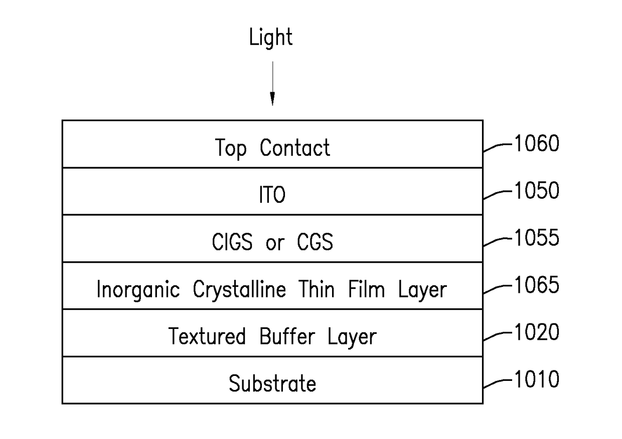
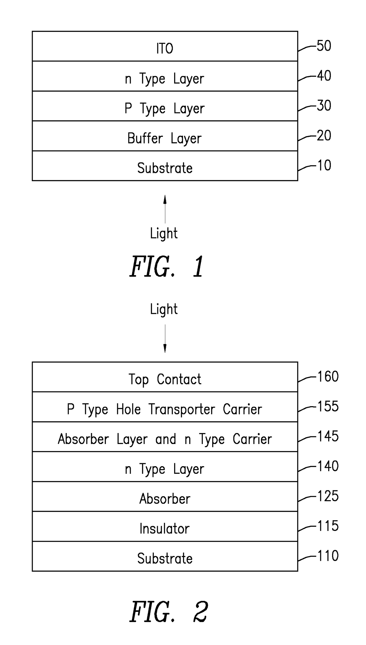
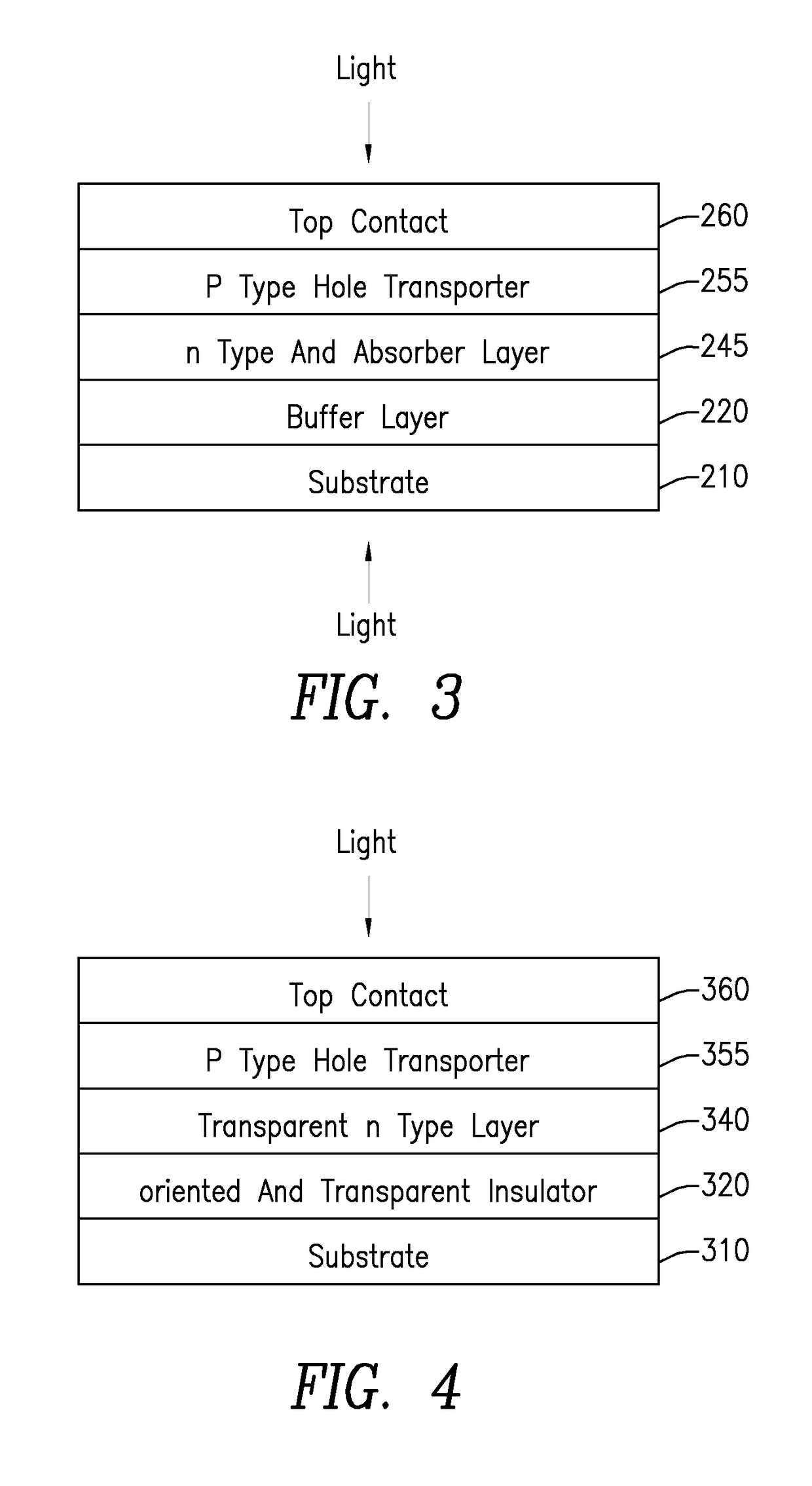
The present invention provides various configurations for a tandem solar cell semiconducting device made up of two thin films. These configurations include variations such as copper oxide / silicon thin film tandem solar cell, perovskite / silicon thin film tandem solar cell, a simple, textured perovskite solar cell, a tandem solar cell with a high bandgap top layer, a tandem cell with a passivation layer, perovskite-perovskite-silicon solar cell, perovskite-perovskite-silicon tandem solar cell, nanowire tandem solar cell, multi junction solar cell configuration, bottom gate transistor, OLED device and a thin film tandem solar cell with CIGS (CGS). These configurations provide improved efficiency and performance of solar cells.

Problems solved by technology

In practice preparing this large area junction successfully and without detriment to material quality is a challenge and limits the number of suitable materials.

Method used


Image

  • High efficiency thin film tandem solar cells and other semiconductor devices
  • High efficiency thin film tandem solar cells and other semiconductor devices
  • High efficiency thin film tandem solar cells and other semiconductor devices

Examples


Embodiment Construction

[0020]The present application discloses architectures for tandem solar consisting of two thin films. Exemplary materials used for the top layer are CIGS (CGS), perovskites (Sn and Ge), amorphous silicon (a-Si), copper oxide, tin sulfide, CZTS and III-V materials. For the bottom layer an inorganic film such as either silicon or germanium may be used. In general, the architecture consists of a glass, plastic or metal substrate (for example, soda-lime or quartz), and a buffer layer, either an oxide insulator or nitride conductor. For electron selector layers (ESL) or hole transport layers (HTL), various materials can be used, such as tin oxide or Spiro-OMeTAD. Transparent conducting oxides (TCO) for top contacts can be indium tin oxide (ITO) or fluorine doped tin oxide (FTO), and the top contacts can be Ag or Au, for example. Various thicknesses of all these materials can be applied, and adjusted or modified according to desired results. However, the thickness of the absorber layers sh...


PUM

PropertyMeasurementUnit
thicknessaaaaaaaaaa
thicknessaaaaaaaaaa
thicknessaaaaaaaaaa

Abstract

Architectures for tandem solar cell including two thin films forming a top layer and a bottom layer. Such cells can be bi-facial. Exemplary materials used for the top layer are CIGS (CGS), perovskites (Sn and Ge), amorphous silicon (a-Si), copper oxide, tin sulfide, CZTS and III-V materials. For the bottom layer an inorganic film such as either silicon or germanium may be used. In general, the architecture includes of a glass, plastic or metal substrate and a buffer layer, either an oxide insulator or nitride conductor.

Description

[0001]This application claims priority to U.S. Provisional Patent Application No. 62 / 345,406 filed Jun. 3, 2016 entitled “Methods of Fabricating Solar Cells” and is hereby incorporated by reference in its entirety.[0002]Solar cells are made of many different kinds of materials, and these materials require a device design that matches their particular qualities if they are to produce electricity from sunlight at their maximum potential. For a real device to approach the limiting efficiency, it should have an optimum energy gap, string light absorption, efficient charge separation and charge transport, and the load resistance should be optimized. Therefore, how a particular solar cell is designed is crucial to its performance and, even if the material engineered is ideal, if the overall device design is not adequate, the solar cell cannot perform well.[0003]US patents and publications by P. Chaudhari and A. Chaudhari (2016 / 0293790; 2016 / 0260863; 2016 / 0322532; 2016 / 0329159; 2016 / 032945...

Claims


Application Information

Patent Timeline
Patent Type & Authority Applications(United States)
IPC IPC(8): H01L51/52H01L31/0236H01L31/0216H01L29/786H01L31/0304H01L31/0224H01L31/0749H01L31/0725H01L31/0352
CPCH01L51/5268H01L31/0725H01L31/02366H01L31/02167H01L29/78678H01L31/0304H01L31/022475H01L31/0749H01L31/035227Y02E10/541H01L31/032H01L31/03365H01L31/0392H01L31/03923H01L31/072H01L31/043H10K30/57H10K50/822H10K2102/321H10K85/50
Inventor CHAUDHARI, ASHOK
Owner SOLAR TECTIC
Learn More