Monolithic microwave integrated circuit (MMIC) and method for forming such mmic having rapid thermal annealing compensation elements

a microwave integrated circuit and compensation element technology, applied in the direction of electrical apparatus, semiconductor devices, semiconductor/solid-state device details, etc., can solve the problems of non-uniform heating profile, inability to meet the requirements of rta system incident infrared energy, and the wafer with respect to incident infrared energy can change significantly, so as to reduce the space required for isolation, increase attenuation, and reduce electrical coupling

Active Publication Date: 2018-02-01
RAYTHEON CO
View PDF6 Cites 0 Cited by
  • Summary
  • Abstract
  • Description
  • Claims
  • Application Information

AI Technical Summary

Benefits of technology

[0011]In one embodiment, the plurality of “dummy” fill provide uniform heating of the substrate during the anneal processing of the substrate.
[0016]More particularly, during the rapid thermal anneal (RTA) of ohmic metal contacts to AlGaN semiconductor material, the heating profile is non-uniform due to the fact that heat transfer is radiative (infrared) and the ohmic metal features are typically not uniformly distributed across an integrated circuit, but residing only in the active device regions of the circuit. This leads to non-uniform alloying across the wafer. Further, establishing an RTA process that works well for one circuit design inevitably leads to variation when applied to another design with differing metal topology because the optical properties (absorption, reflection and transmission) of the wafer with respect to the incident infrared energy from the RTA system can change significantly. As noted above, one solution to this problem is to add “dummy” fill elements in empty spaces (and, in one embodiment, under passive components) of the MMIC. Adding such structures, one can tailor the optical profile of any given wafer, allowing one to significantly reduce heating variation across a wafer and from design to design when utilizing a RTA process. By tailoring optical profile, DC / RF / visual yield, gate leakage current, and morphology of MMIC can be improved and the cost of MMIC / mm2 can be reduced. However, as noted above, adding such structures to a MMIC design may induce unwanted RF performance degradation due to electromagnetic coupling losses between the circuit elements and the “dummy” fill elements. RF performance degradation can take the form of reduced gain, efficiency, output power, noise figure, etc.
[0017]Thus, as noted above, the inventors introduce microwave lossy, material into the “dummy” fill elements which both: improves RTA heating uniformity across any given wafer; and minimizes any deleterious impact to RF performance. Microwave lossy material is used for the “dummy” fill elements to mitigate any undesired electromagnetic coupling from the circuit elements into the “dummy” fill elements, which mitigates any circuit performance impact due to the introduction of the fill elements. Thus, as noted above, here microwave lossy metal “dummy” fill elements are used to simultaneously solve the heating uniformity problem without inducing RF performance degradation in the circuit thereby enabling the area required for the “dummy” fill elements to be closer to the microwave circuit coupled to the FET band freeing up additional surface area on the chip for additional circuitry and / or reducing the cost of MMIC / mm2 even more.
[0018]Thus, the disclosure provides on-wafer compensation elements (“dummy” fill elements) for improved heating uniformity during rapid thermal anneal (RTA) processing, with such elements having electrical properties that allow for improved compaction when integrated with radio frequency (RF) monolithic microwave integrated circuit (MMIC) technology.

Problems solved by technology

More particularly, during the rapid thermal anneal (RTA) of ohmic metal contacts to AlGaN semiconductor material, the heating profile is non-uniform due to the fact that heat transfer is radiative (infrared) and the ohmic metal features are typically not uniformly distributed across an integrated circuit, but residing only in the active device regions of the circuit.
This leads to non-uniform alloying across the wafer.
Further, establishing an RTA process that works well for one circuit design inevitably leads to variation when applied to another design with differing metal topology because the optical properties (absorption, reflection and transmission) of the wafer with respect to the incident infrared energy from the RTA system can change significantly.
However, as noted above, adding such structures to a MMIC design may induce unwanted RF performance degradation due to electromagnetic coupling losses between the circuit elements and the “dummy” fill elements.
RF performance degradation can take the form of reduced gain, efficiency, output power, noise figure, etc.

Method used


Image

  • Monolithic microwave integrated circuit (MMIC) and method for forming such mmic having rapid thermal annealing compensation elements
  • Monolithic microwave integrated circuit (MMIC) and method for forming such mmic having rapid thermal annealing compensation elements
  • Monolithic microwave integrated circuit (MMIC) and method for forming such mmic having rapid thermal annealing compensation elements

Examples


Embodiment Construction

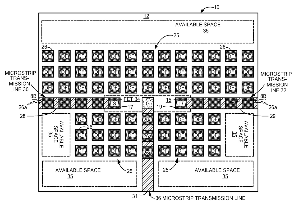
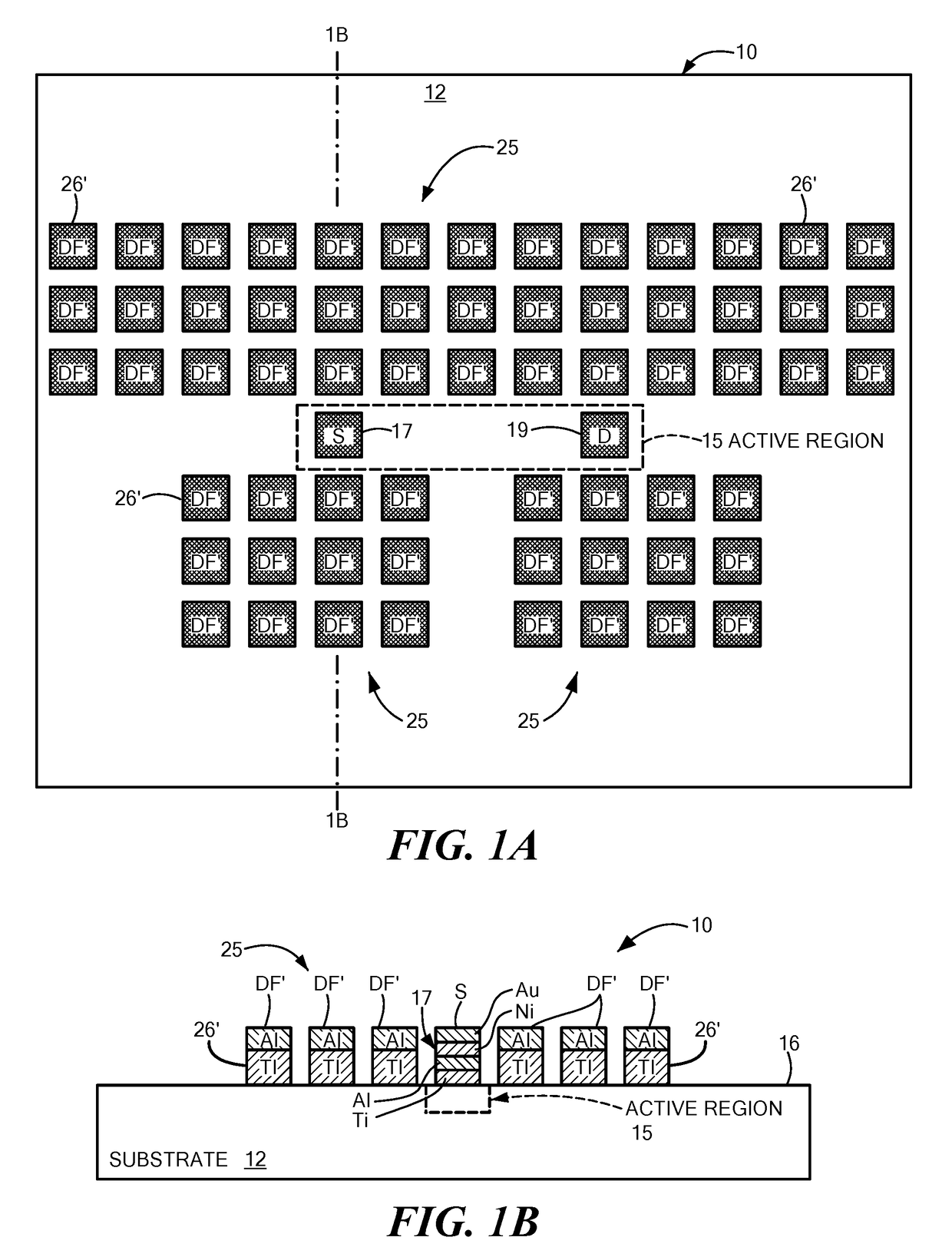
[0030]Referring now to FIGS. 1A and 1B, a Monolithic Microwave Integrated Circuit structure 10 is shown. The structure 10 includes a substrate 12, here for example, silicon carbide (SiC) having an active device region 15, here, for example an aluminum gallium nitride (AlGaN) region on a portion of an upper surface 16 of the substrate 12. The structure 10 includes, on the substrate 12, a source (S) contact material 17 and a drain (D) contact material 19, here for example, a Ti / Al / Ni / Au stack (a bottom layer of titanium, a layer of aluminum of the layer of titanium, a layer of nickel on the layer of aluminum, and a top layer of gold on the layer of nickel) disposed on the active region 15, as indicated. The substrate 12 also includes a plurality of “dummy” fill elements 26′ (also indicated as DF'), here arranged, for example, in three arrays 25 outside of the active region 15, as shown. Here, for example, each one of the “dummy” fill elements 26′ is here a stack of Ti / Al (a bottom lay...


PUM


Abstract

A method and structure, the structure having a substrate, an active device in an active device semiconductor region; of the substrate, a microwave transmission line, on the substrate, electrically connected to the active device, and microwave energy absorbing “dummy” fill elements on the substrate. The method includes providing a structure having a substrate, an active device region on a surface of the structure, an ohmic contact material on the active device region, and a plurality of “dummy” fill elements on the surface to provide uniform heating of the substrate during a rapid thermal anneal process, the ohmic contact material and the “dummy” fill elements having the same radiant energy reflectivity. The rapid thermal anneal processing forms an ohmic contact between an ohmic contact material and the active device region and simultaneously converts the “dummy” fill elements into microwave lossy “dummy” fill elements.

Description

TECHNICAL FIELD[0001]This disclosure relates generally to rapid thermal anneal (RTA), uniform rapid thermal anneal compensation elements, and more particularly to Monolithic Integrated Circuits having RTA uniform compensation elements.BACKGROUND AND SUMMARY[0002]As is known in the art, rapid thermal anneal (RTA) apparatus has been used in the semiconductor industry for many years. Early, the apparatus was used in processing silicon wafers during an implantation activation phase of the fabrication. One such arrangement uses apparatus wherein a silicon wafer is positioned between a set of horizontally disposed upper heating lamps and a set of horizontally disposed lower heating lamps.[0003]In more recent times, RTA apparatus has been used to alloy metals such as when forming ohmic contacts to the active devices, for example, source and drain contacts for Field Effect Transistors (PETS) formed on compound semiconductor materials, such as GaN or GaAs. In some applications, a susceptor, ...

Claims


Application Information

Patent Timeline
Patent Type & Authority Applications(United States)
IPC IPC(8): H01L23/64H01L21/768H01L21/324H01L23/58
CPCH01L23/647H01L23/585H01L2924/1423H01L21/324H01L21/768H01L21/28575H01L21/67115H01L23/66H01L29/812H01L2223/6616H01L23/522H01L23/5225H01L21/2686
Inventor ALTUNKILIC, FIKRETWILLIAMS, ADRIAN D.MACDONALD, CHRISTOPHER J.ALAVI, KAMAL TABATABAIE
Owner RAYTHEON CO
Why Eureka
Try Eureka