Cascode Amplifier Bias Circuits

a cascode amplifier and bias circuit technology, applied in the field of electromechanical circuits, can solve the problems of poor suited circuits, dc supply voltage, etc., and achieve the effects of rapid adaptation to a changing rf electrical environment, poor output resistance characteristics, and good isolation

Active Publication Date: 2018-03-22
PSEMI CORP
View PDF11 Cites 65 Cited by
  • Summary
  • Abstract
  • Description
  • Claims
  • Application Information

AI Technical Summary

Problems solved by technology

While the illustrated cascode circuit provides good isolation because there is no direct coupling from the output to the input, the circuit is not well suited to applications in which the DC supply voltage varies, such as applications where the DC supply voltage at the drain is actively modified to optimize operation at different power levels; examples are average power tracking (APT), envelope tracking (ET), and GSM power amplifier power control.
One problem area for using silicon-based CMOS transistors in cascode amplifier circuits is creating bias circuits, particularly in cases in which the DC supply voltage varies and in the case of amplifiers with a transistor stack height of 3 or more.
Silicon-based CMOS devices with short channel lengths provide fast RF response—a desirable characteristic in an amplifier—but suffer from poor output resistance characteristics due to the influence of the drain voltage on the gate of a transistor device.
As such, they are not amenable to common open-loop bias techniques, such as current mirrors, without suffering from a large and undesirable mismatch between a reference device current and the output device current.
In addition, the problem can be further exasperated in SOS and SOI CMOS technologies due to issues associated with the floating body or “kink” effect.
In the floating body effect, the body of a transistor may form a capacitor with the insulated substrate; charge accumulation on this capacitor may cause the formation of parasitic transistors consuming unwanted parasitic currents and further degrading the output resistance of devices intended to be used as current sources.
Another challenge in designing bias circuits for silicon-based CMOS cascode amplifiers is to configure such circuits so that they are tolerant of supply and bias voltage variations, and bias current variations.
Traditional cascode bias circuits include diode connected devices which do not accommodate a wide range of supply and bias voltages.
Bias current variations may be driven by variations in process, temperature, and voltage (i.e., “PVT” effects), the end result of which is to cause fluctuations in bias current leading to fluctuations in RF performance.
Another drawback to using silicon-based CMOS devices for amplifier applications, and particularly for power amplifier applications, is a relatively low breakdown voltage per device.
Yet another challenge in designing RF amplifiers is that, in many applications, the RF electrical environment of a transmitter, receiver, or transceiver is constantly changing.
A system performance profile that ideally sets such metrics for one situation (such as high gain, moderate linearity, and low noise in the presence of a small received signal) can be completely inappropriate as the RF environment changes (such as with increasing received signal power).
These situation transitions can occur many times during a single usage session of an RF circuit (for example, as a cellular phone moves relative to signal towers), and not adjusting to an appropriate performance profile as the RF environment changes can result in poor or non-functioning RF circuit performance.

Method used


Image

  • Cascode Amplifier Bias Circuits
  • Cascode Amplifier Bias Circuits
  • Cascode Amplifier Bias Circuits

Examples


Embodiment Construction

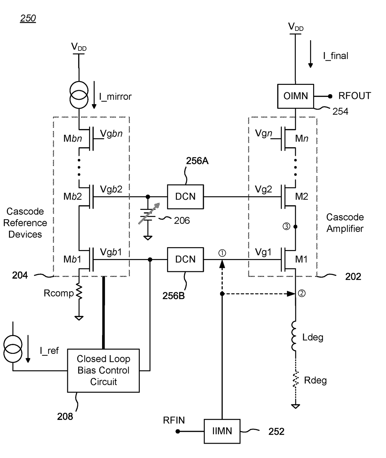
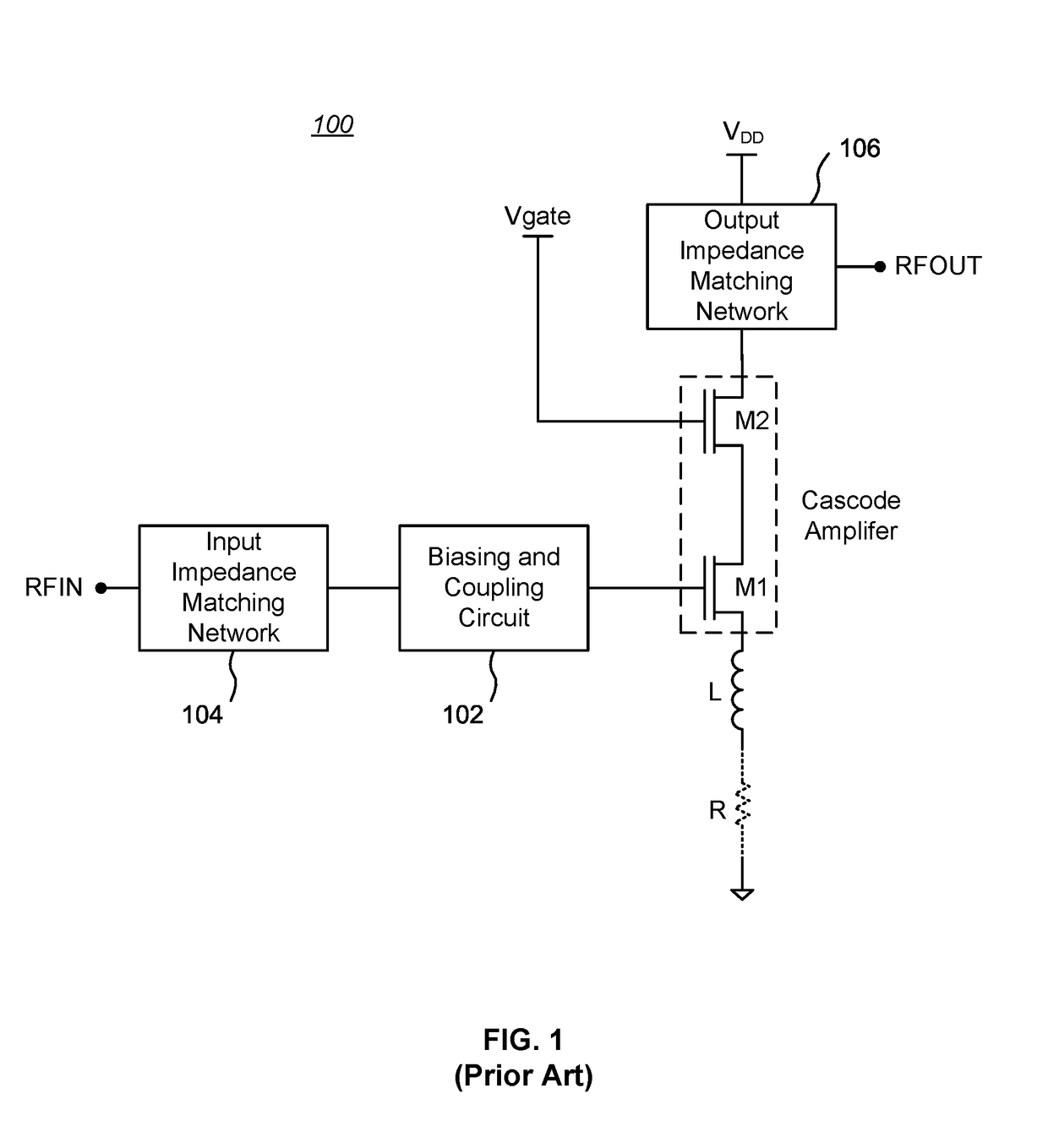
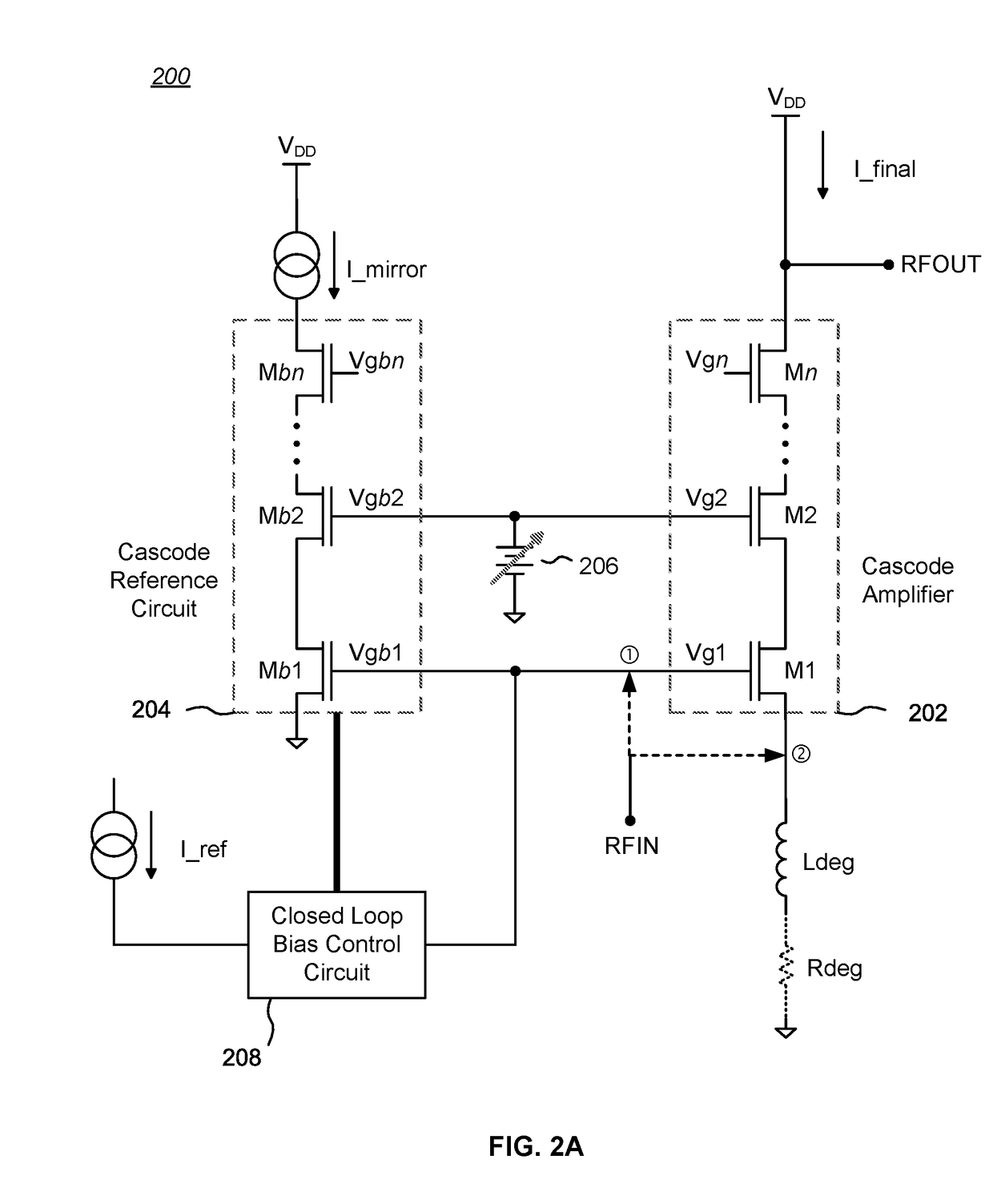
[0029]The invention encompasses bias circuits and methods for silicon-based CMOS amplifier architectures that are tolerant of supply and bias voltage variations, bias current variations, and transistor stack height, and compensate for the poor output resistance characteristics of silicon-based CMOS devices with short channel lengths. Further, the invention encompasses improved silicon-based CMOS amplifier architectures that can rapidly adapt to a changing radio frequency (RF) electrical environment, and which have good isolation. The disclosed amplifier architectures that are adaptable to a number of amplifier applications, including power amplifiers (PAs) and low-noise amplifiers (LNAs).

[0030]Embodiments of the invention utilize a cascode reference circuit to bias the final stages of a cascode amplifier under the control of a closed loop bias control circuit. The closed loop bias control circuit ensures that the current in the cascode reference circuit is approximately equal to a s...


PUM


Abstract

Bias circuits and methods for silicon-based amplifier architectures that are tolerant of supply and bias voltage variations, bias current variations, and transistor stack height, and compensate for poor output resistance characteristics. Embodiments include power amplifiers and low-noise amplifiers that utilize a cascode reference circuit to bias the final stages of a cascode amplifier under the control of a closed loop bias control circuit. The closed loop bias control circuit ensures that the current in the cascode reference circuit is approximately equal to a selected multiple of a known current value by adjusting the gate bias voltage to the final stage of the cascode amplifier. The final current through the cascode amplifier is a multiple of the current in the cascode reference circuit, based on a device scaling factor representing the relative sizes of the transistor devices in the cascode amplifier and in the cascode reference circuit.

Description

CROSS-REFERENCE TO RELATED APPLICATIONS[0001]The present application is related to U.S. application Ser. No. ______ entitled “Standby Voltage Condition for Fast RF Amplifier Bias Recovery” (Attorney Docket No. PER-195-PAP) filed on even date herewith, the disclosure of which is incorporated herein by reference in its entirety. The present application is also related to U.S. application Ser. No. ______ entitled “Gate Drivers for Stacked Transistor Amplifiers” (Attorney Docket No. PER-194-PAP) filed on even date herewith, the disclosure of which is incorporated herein by reference in its entirety. The present application is also related to U.S. application Ser. No. ______ entitled “Body Tie Optimization for Stacked Transistor Amplifier” (Attorney Docket No. PER-199-PAP) filed on even date herewith, the disclosure of which is incorporated herein by reference in its entirety.[0002]The present application may be related to U.S. Pat. No. 7,248,120, issued on Jul. 24, 2007, entitled “Stack...

Claims


Application Information

Patent Timeline
Patent Type & Authority Applications(United States)
IPC IPC(8): H03F1/22H03F1/30H03F1/56H03F3/193
CPCH03F1/223H03F1/301H03F1/56H03F3/193H03F2200/451H03F2200/387H03F2200/18H03F2200/102H03F2200/105H03F2200/222H03F3/195H03F3/213H03F3/245H03F2200/165H03F2200/21H03F2200/225H03F2200/243H03F2200/294H03F2200/297H03F2200/301H03F2200/306H03F2200/391H03F2200/399H03F2200/42H03F2200/48H03F2200/489H03F2200/492H03F2200/498H03F2200/555H03F2200/61H03F2200/78
Inventor KLAREN, JONATHANWAGH, POOJANKOVAC, DAVIDSHAPIRO, ERIC S.CALANCA, NEILNOBBE, DAN WILLIAMMURPHY, CHRISTOPHERENGLEKIRK, ROBERT MARKAYRANCI, EMREBARGROFF, KEITHRANTA, TERO TAPIO
Owner PSEMI CORP
Why Eureka
Try Eureka