Optical sensing with critically coupled planar waveguide with optional integration of layered two-dimensional materials

a planar waveguide and optical sensing technology, applied in the field of optical sensing, can solve the problems of difficult scale-up of prefabricated electrode arrays, lack of flexibility to measure electrical fields at arbitrary spatial positions, and little research into label-free optical platforms that permit spatio-temporal detection of electric fields

Active Publication Date: 2018-04-19
RGT UNIV OF CALIFORNIA
View PDF5 Cites 9 Cited by
  • Summary
  • Abstract
  • Description
  • Claims
  • Application Information

AI Technical Summary

Problems solved by technology

However, it remains an outstanding challenge to achieve label-free, nonperturbativedetection with high field sensitivity and high spatio-temporal resolution.
These techniques require prefabricated electrode arrays that are difficult to scale up, are individually amplified, and do not provide the flexibility to measure electrical fields at arbitrary spatial positions.
Despite these advantages, there is little research into label-free optical platforms that permit the spatio-temporal detection of electric field22 distributions.
Understanding the information transmitted through electric field distributions in biological systems is one of the major problems in both physiology and behavioral neurology.
Finding a method to extract all information in the intercellular electrical activity is difficult, and current techniques such as multielectrode and multitransistor arrays, calcium imaging, and voltage-sensitive dye fluorescence have limitations.
Some of the intrinsic properties of SPRs limit their performance.
(1) The sensitivity of an SPR sensor is intrinsically limited by the large absorption losses of metals at optical frequencies.
The damping of metal broadens the resonance linewidth and sets an ultimate sensitivity limit.
(2) The SPR dispersion is determined by the properties of metals, therefore one cannot arbitrarily tune the probing wavelength or incident angle.
(3) SPR signals vary with temperature sensitively which causes problems when the sample temperature is not stable or when a temperature dependence is considered.

Method used


Image

  • Optical sensing with critically coupled planar waveguide with optional integration of layered two-dimensional materials
  • Optical sensing with critically coupled planar waveguide with optional integration of layered two-dimensional materials
  • Optical sensing with critically coupled planar waveguide with optional integration of layered two-dimensional materials

Examples


first embodiment

ritical Coupling Condition

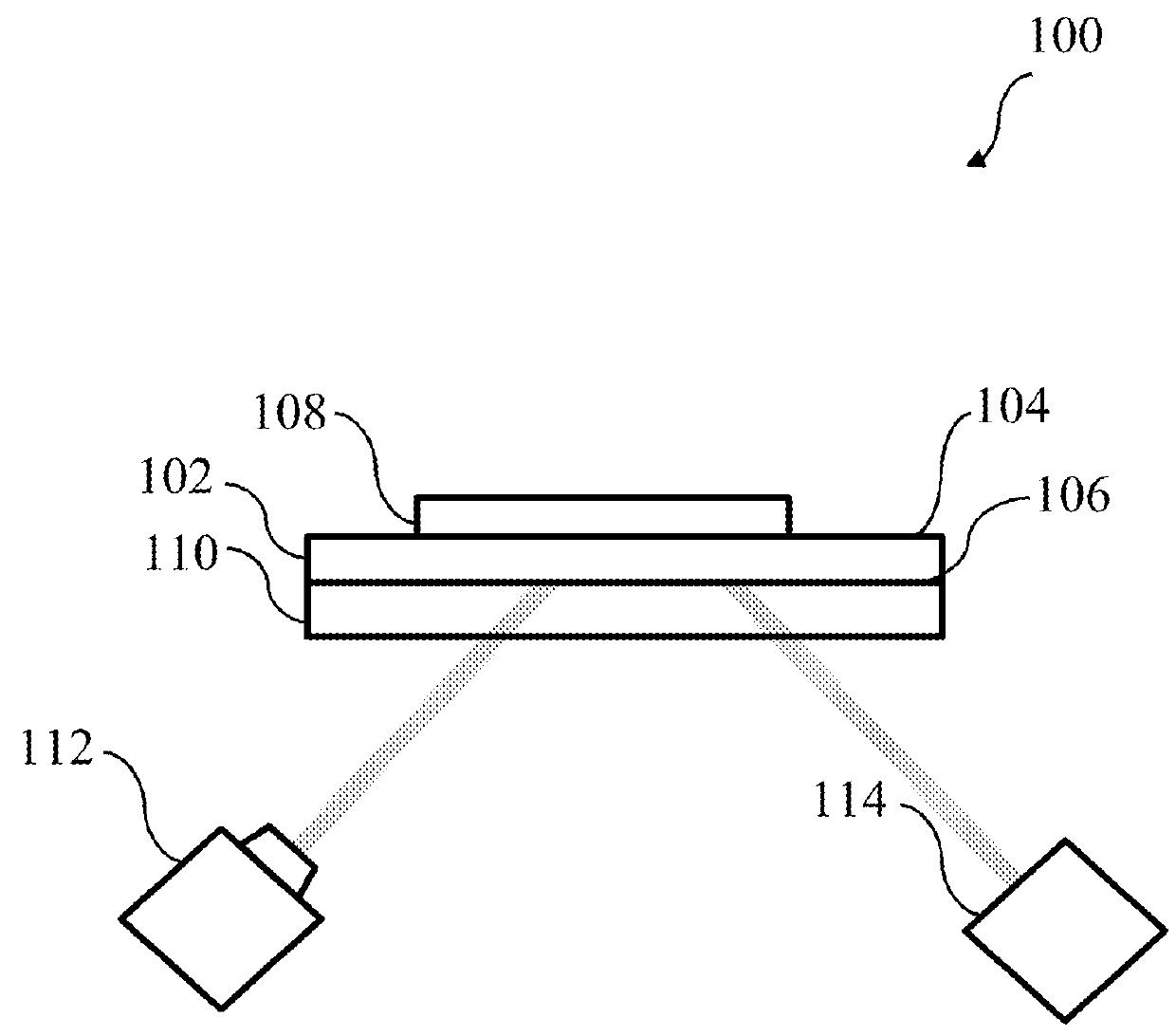
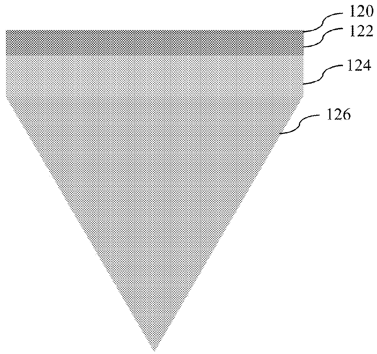
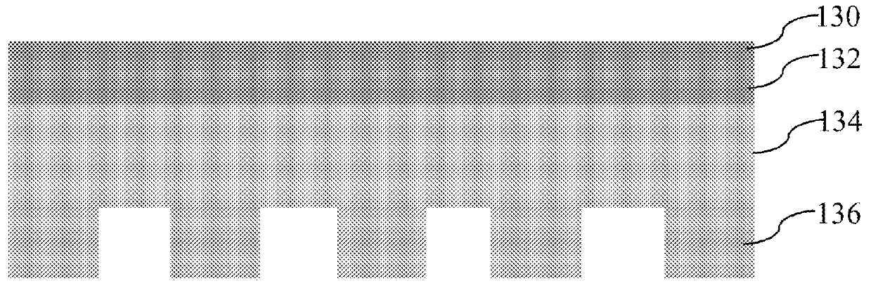
[0059]Some embodiments of the invention pair the optical critical coupling condition with a planar waveguide for a versatile and high sensitivity optical sensing platform at two-dimensional surfaces and interfaces. In this scheme, an absorptive sheet of two-dimensional material is deposited on the planar waveguide as the functional layer. The thickness of coupling layer, which determines the coupling efficiency through frustrated total internal reflection, is fine-tuned to achieve the so-called critical coupling condition. The light can be efficiently absorbed by the functional layer under the critical coupling condition, which leads to minimal reflectance from the planar waveguide. A modification of absorption in the functional layer due to environmental perturbation breaks the critical coupling condition and leads to a greatly enhanced optical signal. The sensor operating near to the critical coupling condition can be tailored to have excellent sensitivit...

example 1

Electric Field Sensor

[0064]Signaling and manipulation through the control of electric field distributions is ubiquitous to both biological and physical systems. For example, intercellular electrical activity is central to the signaling and computation of excitable cells such as cardiac and neuronal cells. The voltages generated by bio-electric fields span three orders of magnitude and can fluctuate on the scale of microseconds to hours.8,9 Likewise, the generation and manipulation of electric fields inside microscopic channels is the backbone of microfluidics and lab-on-a-chip diagnostics.10,11

[0065]Optical absorptions of many two-dimensional materials, such as graphene and transition metal dichalcogenides, can be modulated through electrostatic potential. This makes two-dimensional materials ideal as the functional layer for electric field sensing because 1) the optical absorption can change due to a local electric potential difference in the target material, and 2) the optical ab...

example 2

-Resolved Imaging Using Other 2D Materials

[0114]A two-dimensional optical sensing platform according to some embodiments of the invention combines unprecedented sensitivity with the capability of two-dimensional optical imaging and high-speed dynamic detection. This platform makes use of a two-dimensional planar waveguide close to the critical coupling conditions, and with the possibility to integrate with layered two-dimensional materials for extended sensing capabilities. It allows for high speed, high sensitivity, and high throughput sensing of a wide range of stimulants, such as chemical and biological adsorbates, electrical fields, PH, and strain, at two-dimensional interfaces.

[0115]Some embodiments of the invention combine many desirable features in one platform, including high sensitivity, ease of use, high parallel detection with two-dimensional imaging, high-speed operation, and flexibility for detecting different physical parameters. In comparison, electrical detection bas...


PUM

PropertyMeasurementUnit
thicknessaaaaaaaaaa
voltage sensitivityaaaaaaaaaa
surface areaaaaaaaaaaa

Abstract

An optical sensing system includes a planar optical waveguide having a first surface for detection and a second surface for coupling light. The optical sensing system includes a functional layer integral with the first surface of the planar optical waveguide, and a coupling layer in contact with the second surface of the planar optical waveguide, the coupling layer having a lower refractive index than the planar optical waveguide. The optical sensing system includes an optical source arranged to illuminate at least a portion of the second surface of the planar optical waveguide through the coupling layer with substantially critical optical coupling. The optical sensing system also includes an optical detector arranged to receive a portion of light from the optical source after being reflected from the first surface of the planar optical waveguide and passing through the coupling layer.

Description

[0001]This application claims priority to U.S. Provisional Application No. 62 / 307,369 filed Mar. 11, 2016, the entire content of which is hereby incorporated by reference.[0002]This invention was made with U.S. Government support under Grant No. 1344302, awarded by the National Science Foundation. The Government has certain rights in the invention.BACKGROUND1. Technical Field[0003]The field of the currently claimed embodiments of this invention relates to optical sensing, and more particularly to optical sensing with a critically coupled planar waveguide.2. Discussion of Related Art[0004]Signaling and manipulation through the control of electric field distributions is ubiquitous to both biological and physical systems. For example, intercellular electrical activity is central to the signaling and computation of excitable cells such as cardiac and neuronal cells.7 The voltages generated by bio-electric fields span three orders of magnitude and can fluctuate on the scale of microsecon...

Claims


Application Information

Patent Timeline
Patent Type & Authority Applications(United States)
IPC IPC(8): G01N21/552G01N21/77G01N21/33G01N21/3563
CPCG01N21/554G01N21/7743G01N21/33G01N21/3563G01N21/41G01N21/552G01R29/0885G01N2021/436G01R19/155G01R29/14
Inventor WANG, FENGHORNG, JASONBALCH, HALLEH B.
Owner RGT UNIV OF CALIFORNIA
Why Eureka
Try Eureka