Dispersion

a technology of dispersion and coating, applied in the field of dispersion, can solve the problems of difficult to form fine wirings by printing methods, difficult to form conductive thin films on low heat-resistant base materials, and conventional circuit board production methods, and achieve excellent reverse printing suitability and smooth coating films.

Active Publication Date: 2018-06-21
ASAHI KASEI KK
View PDF0 Cites 9 Cited by
  • Summary
  • Abstract
  • Description
  • Claims
  • Application Information

AI Technical Summary

Benefits of technology

[0060]Firstly, according to the invention, it is possible to obtain a dispersion including particles that contain one or more selected from the group consisting of metals and metal oxides, and having excellent reverse printing suitability, coated film smoothness, dispersibility and long-term storage stability.
[0061]Secondly, according to the invention, it is possible to obtain a dispersion that can form a low-resistance conductive thin-film without producing high temperature-induced damage in a low-heat-resistance base material.

Problems solved by technology

However, the conventional circuit board production method is disadvantageous in that it has many steps and is complex, while also requiring a photoresist material.
However, the following two problems often arise with printing methods.
First, it is generally difficult to form fine wirings by printing methods.
Second, in a printing method, it is difficult to form a conductive thin-film on a low heat-resistant base material because of the need for a high-temperature firing step to impart conductivity to the print pattern.
When a dispersion containing large-sized particles is used as an ink for printing, the edges and surface of the coated film are rough, and fine patterning cannot be achieved.
When the coated film surface roughness is high, it can have an adverse effect on the properties of the material printed as a layer on the coated film, and therefore the smoothness of the coated film is important.
However, sub-femtoliter ink jet printing has a very slow printing speed and is therefore unsuitable as a technique for mass production.
Moreover, PTL 1 does not disclose any specific strategy for improving the dispersibility and long-term storage stability.
In PTL 2, however, no specific dispersion composition is disclosed for improving the long-term storage stability of the dispersion and the smoothness of the coated film.
With the technique of PTL 5, however, since the base material is subjected to a high temperature of 160° C. or higher during the firing, it is not possible to form copper thin-films on base materials such as polyethylene terephthalate (PET) films, which are very inexpensive but have low heat resistance.
That is, because an expensive base material must be used for application of the technique of PTL 5, it has not been possible to provide an economical printing device.

Method used


Image

  • Dispersion
  • Dispersion
  • Dispersion

Examples


application examples

[Application Examples of the Invention]

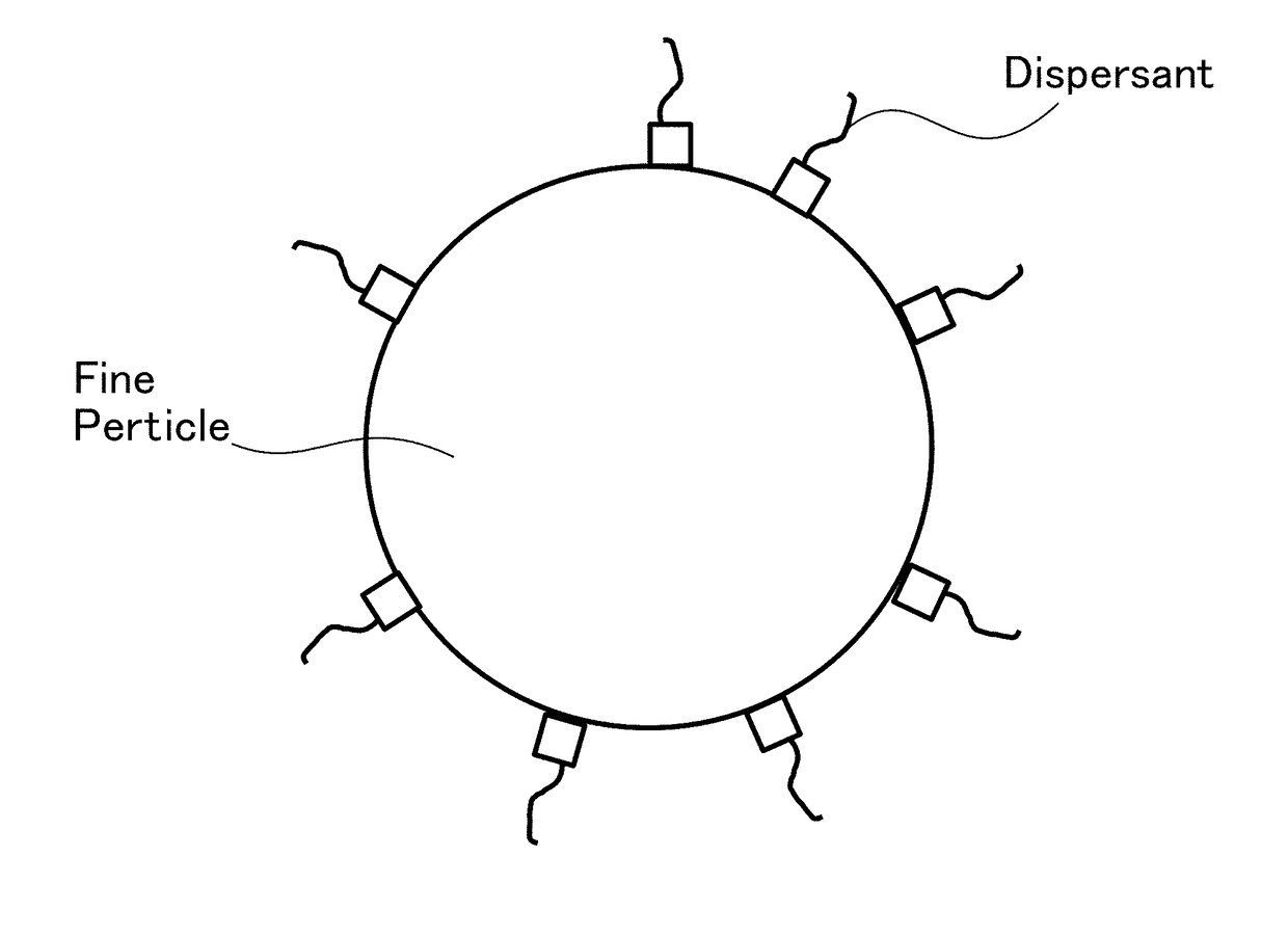
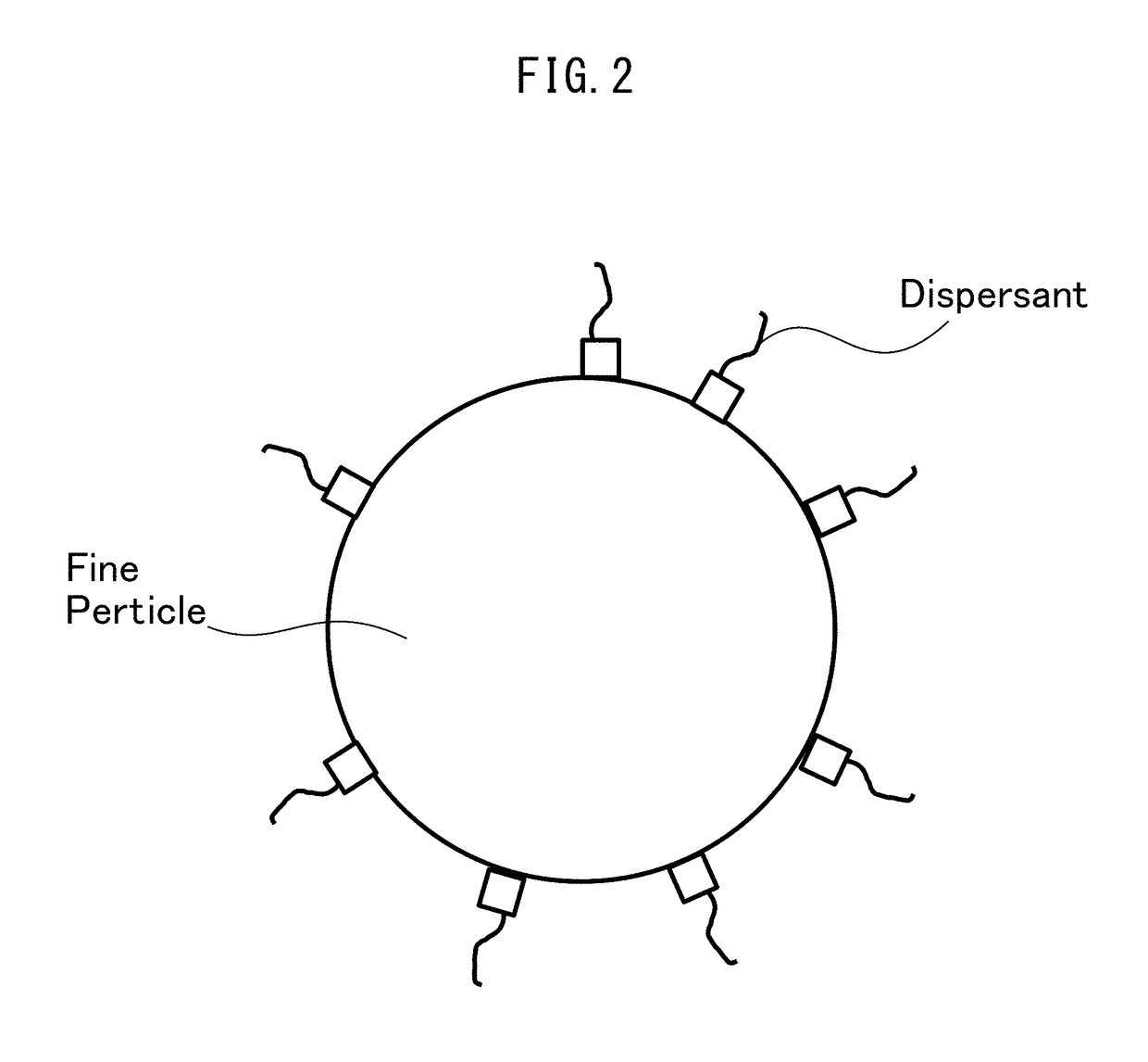
[0309]As explained above, according to this embodiment it is possible to obtain a highly smooth conductive film having a micronized pattern. The conductive film can be satisfactorily utilized in a printed board, flexible printed board, electromagnetic shield sheet, semiconductor device (thin-film transistor, diode or ferroelectric memory) or metal mesh transparent conductive film, for example.

[0310]Application of this embodiment to a metal mesh transparent conductive film will now be explained.

[0311]A metal mesh transparent conductive film is one having a metal wiring with a width of 50 μm or smaller formed in a mesh-like manner on a transparent base material. The metal mesh transparent conductive film has the feature of being apparently transparent but with low electrical resistance on the surface. Since a structure having a width of 50 μm or smaller is poorly visible, the metal wiring of a metal mesh transparent conductive film appears not to...

example 1-13

[0338]To 0.20 g of silver nanopowder with a particle size of <150 nm (product name: “Silver nanopowder, particle size: <150 nm, 99% trace metal basis”, product of Aldrich) there were added a mixture of 0.010 g of poly(ethylene glycol) methyl ether thiol with a number-average molecular weight of 6,000 (product of Aldrich Co.) and 0.030 g of poly(ethylene glycol) methyl ether thiol with a number-average molecular weight of 800 (product of Aldrich Co.), as a dispersant, and 0.76 g of distilled water as a solvent, and a homogenizer was used for dispersion to obtain a dispersion for Example 1-13 containing silver particles.

[0339]The mean secondary particle size of the microparticles in the dispersion of Example 1-13 was 521 nm.

examples 1-14 to 1-16

[0340]Dispersions for Examples 1-14 to 1-16 each containing silver particles were obtained by the same procedure as Example 1-13, except for changing the type and amount of each component in the dispersant mixture, as shown in Table 1.

[0341]Each of the dispersions obtained in Examples 1-13 to 1-16 were measured by GPC, and in the molecular weight distribution curve in terms of polyethylene glycol, a peak was detected in both the molecular weight region of 31 or greater and less than 1,000 and the molecular weight region of 1,000 or greater and 40,000 or less.

[0342]The mean secondary particle sizes of the particles in the dispersions, and the results of the evaluations conducted by the methods described above, are also shown in Table 1.

TABLE 1DispersionParticleMeanCoated filmsecondaryDispersantSolventProlongedFineSurfaceparticleMolecularAmountAmountDispers-storageprintingroughnessTypesize (nm)Typeweight(g)Type(g)ibilitystabilityproperty(nm)Comp.Copper (I)35PEG-MET 8008000.040N-butano...


PUM

PropertyMeasurementUnit
molecular weight distributionaaaaaaaaaa

Abstract

A dispersion which contains a dispersant and particles selected from among metal particles and metal oxide particles, and which is characterized in that: the dispersant has a chemical structure that is able to be bonded or adsorbed to the particles; and the dispersant contains a low-molecular-weight dispersant that has at least one peak within a molecular weight region of 31 or more but less than 1,000 in the molecular weight distribution curve in terms of polyethylene glycol as determined by gel permeation chromatography and a high-molecular-weight dispersant that has at least one peak within a molecular weight region of 1,000 or more but 40,000 or less in the above-described molecular weight distribution curve.

Description

TECHNICAL FIELD[0001]The present invention relates to a dispersion.BACKGROUND ART[0002]Circuit boards have a structure with conductive wiring formed on a substrate. Such circuit boards have conventionally been produced by a process in which a photoresist coated onto a metal foil-attached substrate is worked into a desired negative-type circuit pattern by exposure and development, and then the metal foil at the sections not coated with the resist is removed by chemical etching to form a pattern. By such a conventional method for producing circuit boards it is possible to produce high performance conductive substrates. However, the conventional circuit board production method is disadvantageous in that it has many steps and is complex, while also requiring a photoresist material.[0003]There has been much interest in methods that employ a process of directly printing a desired wiring pattern on a substrate using a coating material dispersing microparticles selected from the group consi...

Claims


Application Information

Patent Timeline
Patent Type & Authority Applications(United States)
IPC IPC(8): C09D5/24C09D7/45C09D171/02C09D7/40H01B5/14H01B13/00H01B1/22B22F1/0545B22F1/102
CPCC09D5/24C09D7/45C09D171/02C09D7/67C09D7/68H01B5/14H01B13/0036H01B1/22C08K2003/0806C08K2201/001C08K2201/005C08K2201/011C08K2003/2248H05K1/092C08K3/08C08K3/22C09D17/00C09D201/00C08L71/02H01B13/00C09D7/40H05K1/097H05K3/1283H05K2201/0269B22F2007/047B22F7/04B22F1/0545B22F1/102B22F1/147C09D17/006C09D17/007H05K1/09H05K3/12
Inventor OOI, HIROTAKAOHNO, EIICHI
Owner ASAHI KASEI KK
Why Eureka
Try Eureka