Organic electroluminescent material
an electroluminescent material and organic technology, applied in the field of organic optoelectronic materials, can solve the problems of high cost of oleds, and achieve the effect of higher color purity
- Summary
- Abstract
- Description
- Claims
- Application Information
AI Technical Summary
Benefits of technology
Problems solved by technology
Method used
Image
Examples
embodiment 1
Compound 1
[0037]
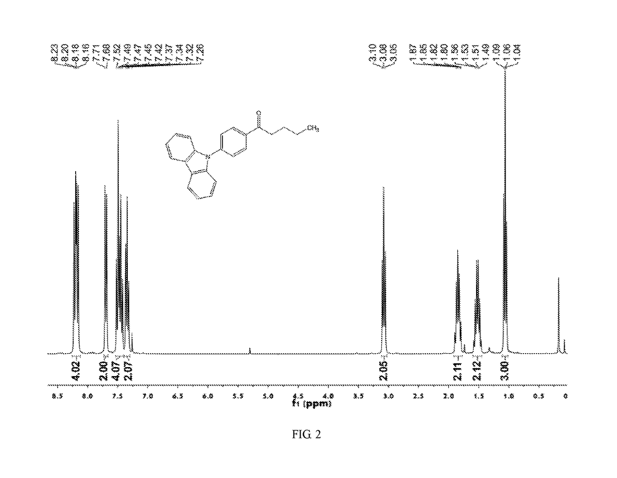
[0038]To a reaction vessel, add 2 g (0.018 mol) of dimethylcarbamoyl chloride and 20 ml of tetrahydrofuran solvent, then oxygen purging and nitrogen protection is performed for the device. Cool down the temperature of the reaction solution to −75˜−65° C. slowly add 10 ml of 1.6M n-BuLi / THF solution dropwise, to control the temperature of the reaction solution at −75˜−65° C. After dripping, continue to maintain this temperature to react 0.5-1 h. After the addition of 6 g of compound 1-1, control the temperature of the reaction solution at −75˜−65° C. After dripping, continue to maintain this temperature to react 0.5-1 h, then transfer the reaction solution to room temperature and naturally heat 4-6 h, then stop the reaction. Add ethyl acetate / deionized water to extract and extract the aqueous layer with ethyl acetate. Combine the organic layer, dry with anhydrous magnesium sulfate, filter, concentrate the filtrate to get an off-white solid. Conduct chromatography for ...
embodiment 2
Example of the Compound in the Invention
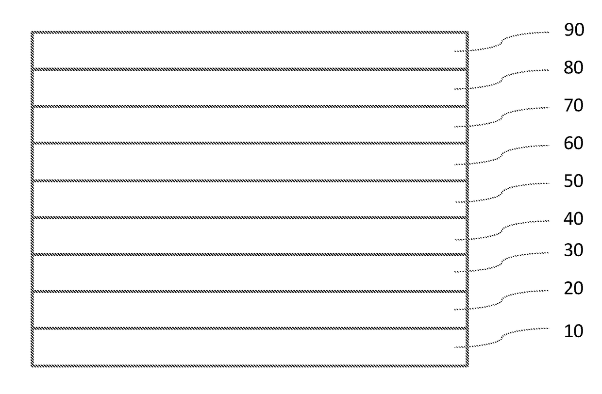
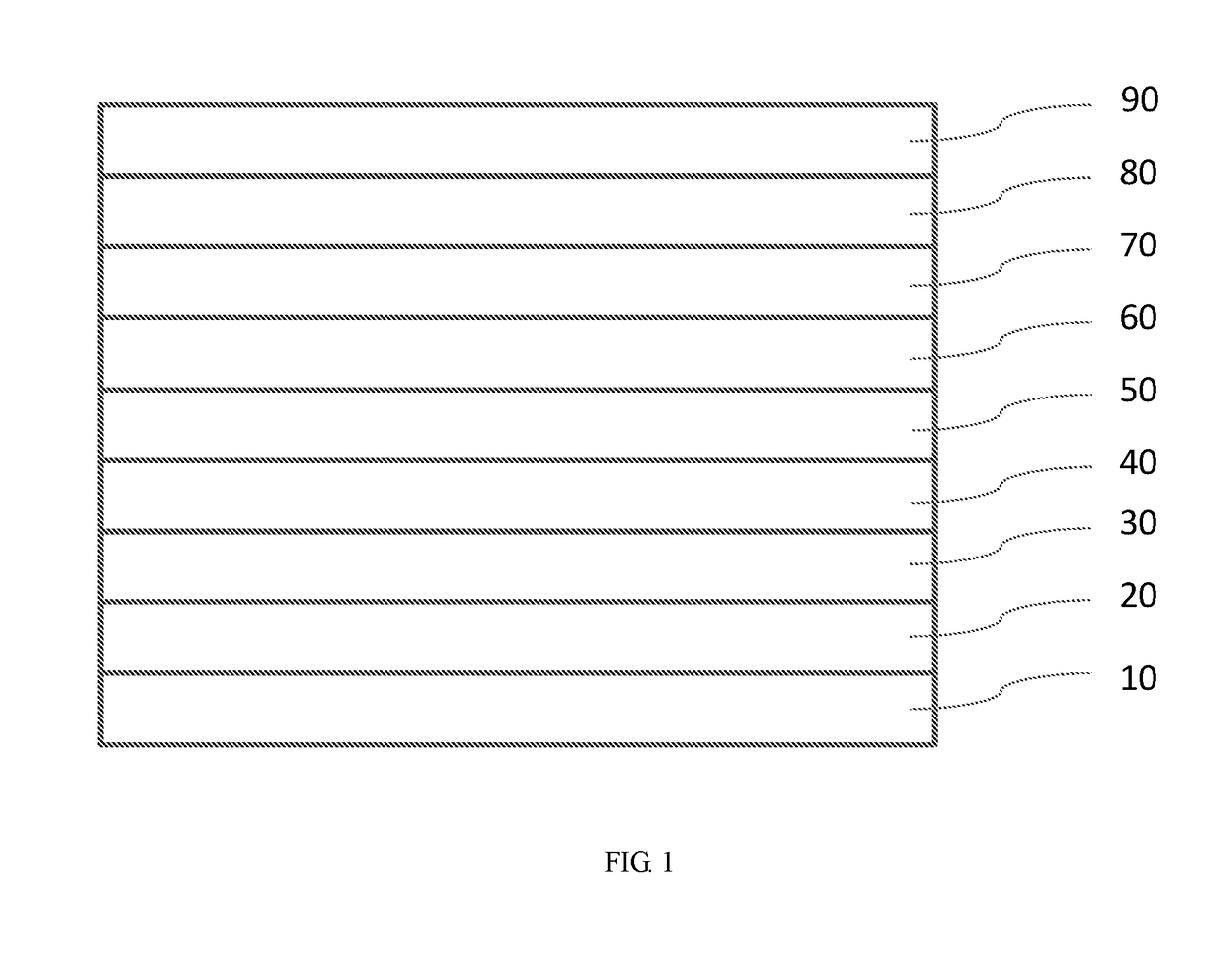
[0039]The device structure is shown in FIG. 1.
[0040]Device Preparation:
[0041]Firstly, the ITO transparent conductive glass substrate 10 (with anode 20 above) is washed with detergent solution and deionized water, acetone ultrasound, isopropanol vapor, and then treated with oxygen plasma for 5 minutes.
[0042]Then, perform vacuum evaporation of 35 nm NPB in ITO, which is used as the hole injection layer 30.
[0043]Then, perform vacuum evaporation of 5 nm of mCP as the electron / exciton blocking layer 40.
[0044]Then, perform vacuum evaporation of 20 nm of light-emitting layer 50, using mCP as a host material and compound 1 in the invention as a doped material, with a doping concentration of 3%.
[0045]Then, perform vacuum evaporation of 10 nm of mCP as the exciton blocking layer 60.
[0046]Then, perform vacuum evaporation of 30 nm of TPBi as the electron transport layer 70.
[0047]Finally, perform vacuum evaporation of 1 nm of LiF as the electron injection ...
PUM
| Property | Measurement | Unit |
|---|---|---|
| emission wavelength | aaaaa | aaaaa |
| emission wavelength | aaaaa | aaaaa |
| electronic luminescent | aaaaa | aaaaa |
Abstract
Description
Claims
Application Information


