Normally-off HEMT transistor with selective generation of 2deg channel, and manufacturing method thereof

Active Publication Date: 2018-12-13
STMICROELECTRONICS SRL
View PDF0 Cites 2 Cited by
  • Summary
  • Abstract
  • Description
  • Claims
  • Application Information

AI Technical Summary

Problems solved by technology

However, this solution has drawbacks due to low electron mobility in the region below the gate region, and poor reliability of the gate dielectric owing to possible breakdowns caused by high electrical fields be

Method used


Image

  • Normally-off HEMT transistor with selective generation of 2deg channel, and manufacturing method thereof
  • Normally-off HEMT transistor with selective generation of 2deg channel, and manufacturing method thereof
  • Normally-off HEMT transistor with selective generation of 2deg channel, and manufacturing method thereof

Examples


Embodiment Construction

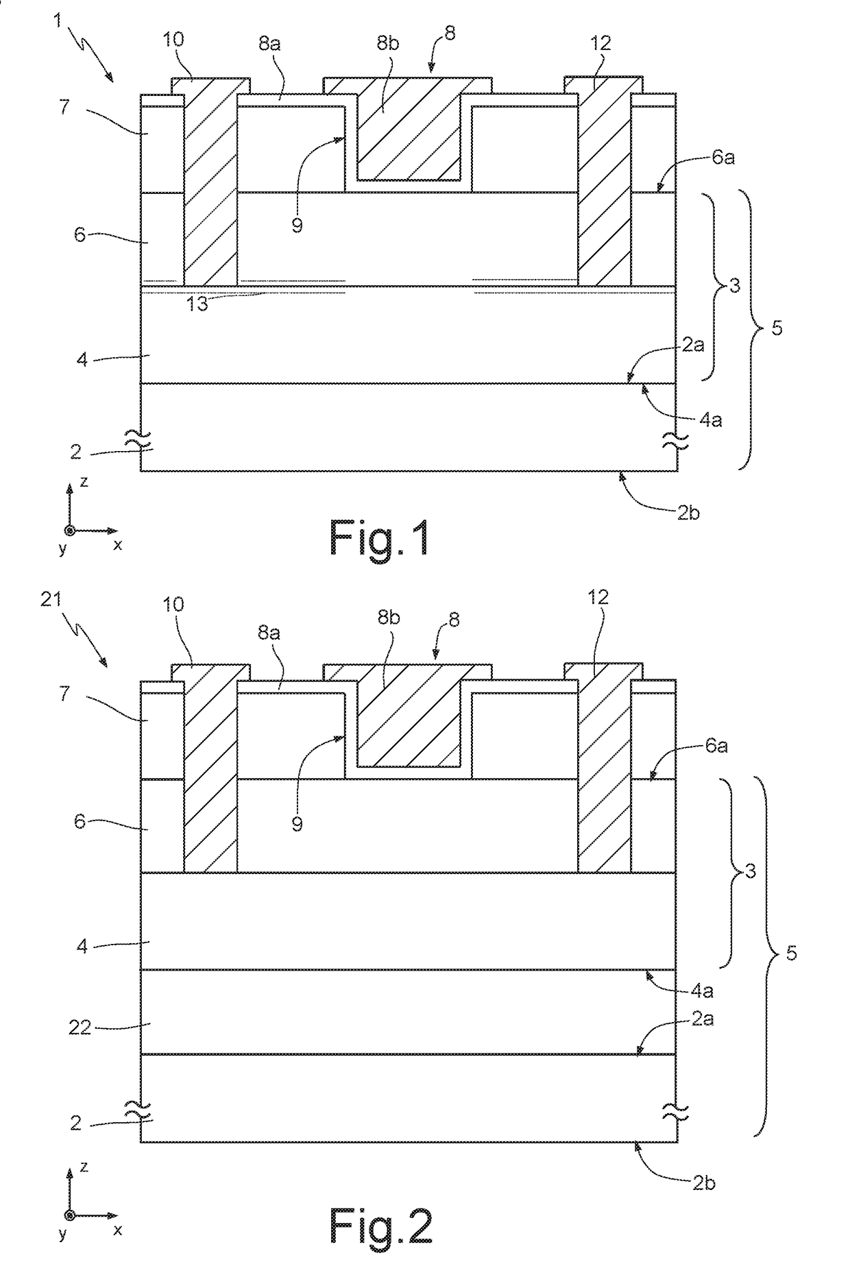
[0017]FIG. 1 shows, in a three-axis system having axes X, Y, Z orthogonal to one another, a normally-off HEMT device 1 including a substrate 2, made for example of silicon or silicon carbide (SiC) or sapphire (Al2O3); a channel layer 4, of intrinsic gallium nitride (GaN), extending over the substrate 2 and having a thickness in the range from about 1 μm to 5 μm; a barrier layer 6, of intrinsic aluminum gallium nitride (AlGaN) or, more generally, of compounds based on ternary or quaternary alloys of gallium nitride, such as AlxGa1-xN, AlInGaN, InxGa1-xN, AlxIn1-xAl, extending over the channel layer 4 and having a thickness tb in the range from about 5 nm to 30 nm; an insulation layer 7, of dielectric material such as nickel oxide (NiO), extending on an upper side 6a of the barrier layer 6; and a gate region 8 extending into the insulation layer 7 between a source region 10 and a drain region 12.

[0018]The channel layer 4 and the barrier layer 6 form a heterostructure 3. The substrate ...


PUM


Abstract

A normally-off HEMT transistor includes a heterostructure including a channel layer and a barrier layer on the channel layer; a 2DEG layer in the heterostructure; an insulation layer in contact with a first region of the barrier layer; and a gate electrode through the whole thickness of the insulation layer, terminating in contact with a second region of the barrier layer. The barrier layer and the insulation layer have a mismatch of the lattice constant (“lattice mismatch”), which generates a mechanical stress solely in the first region of the barrier layer, giving rise to a first concentration of electrons in a first portion of the two-dimensional conduction channel which is under the first region of the barrier layer which is greater than a second concentration of electrons in a second portion of the two-dimensional conduction channel which is under the second region of the barrier layer.

Description

BACKGROUNDTechnical Field[0001]The present disclosure relates to a normally-off high electron mobility field effect transistor (“high electron mobility transistor”, or HEMT), and to a method for manufacturing the HEMT transistor. In particular, the present disclosure relates to a normally-off HEMT transistor incorporating an epitaxial layer of nickel oxide.Description of the Related Art[0002]There are known high electron mobility field effect transistors (“high electron mobility transistors”, or HEMT) based on the formation of high-mobility two-dimensional electron gas (2DEG) layers at a heterojunction, that is to say at the interface between semiconductor materials having different band gaps. For example, there are known HEMT transistors based on the heterojunction between a layer of aluminum gallium nitride (AlGaN) and a layer of gallium nitride (GaN).[0003]HEMT transistors based on AlGaN / GaN heterojunctions offer a number of advantages which makes them particularly suitable and w...

Claims


Application Information

Patent Timeline
IPC IPC(8): H01L29/778H01L29/20H01L29/423H01L29/66H01L29/10
CPCH01L29/7786H01L29/2003H01L29/4236H01L29/66462H01L29/1066H01L29/7378H01L29/778H01L23/291H01L29/41766H01L29/1087H01L29/207H01L23/3171
Inventor IUCOLANO, FERDINANDOGRECO, GIUSEPPEROCCAFORTE, FABRIZIO
Owner STMICROELECTRONICS SRL
Why Eureka
Try Eureka