

Method of evaluating insulated-gate semiconductor device
a technology of insulated-gate semiconductors and semiconductor devices, which is applied in the direction of semiconductor/solid-state device testing/measurement, instruments, scanning probe techniques, etc., can solve the problems of insufficient field-effect mobility that can be achieved, and achieve the effect of increasing the number of summits, high field-effect mobility, and increasing the density of summits
- Summary
- Abstract
- Description
- Claims
- Application Information
AI Technical Summary
Benefits of technology
Problems solved by technology
Method used
Image

Examples
embodiment 1
[0034]
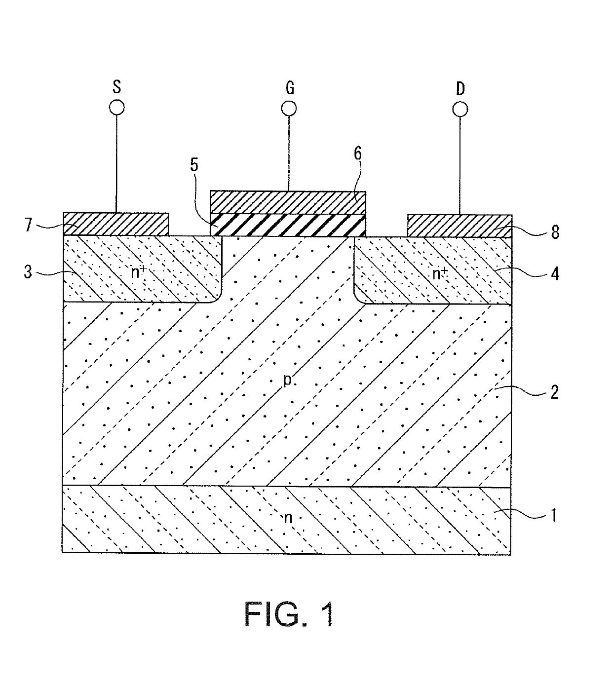
[0035]As illustrated in FIG. 1, an insulated-gate semiconductor device manufactured in Embodiment 1 of the present invention is a MOSFET including an n-type SiC semiconductor substrate 1 and a p-type SiC channel formation layer 2 formed on the semiconductor substrate 1. A high-impurity concentration n-type (n+) source region 3 and a high-impurity concentration n-type (n+) drain region 4 separated from the source region 3 are respectively selectively formed in an upper portion of the channel formation layer 2. The structure illustrated in FIG. 1 is only an example. The channel formation layer 2 may be a well region or the like embedded in an upper portion of the semiconductor substrate 1, or a p-type semiconductor substrate may be used as-is as the channel formation layer 2. Furthermore, in the structure illustrated in FIG. 1, a low-impurity concentration n-type drift region may be formed sandwiched between the channel formation layer 2 and the drain region 4.
[0036]A gate insul...
working example 1
[0068]In Working Example 1, a 4H—SiC substrate having the principal surface of (1-100) is used. The principal surface will be set similarly in other working examples that will be described later. During manufacture of the insulated-gate semiconductor device according to Working Example 1 of Embodiment 1, an inductively coupled plasma (ICP) etching process was used in step (c) for reducing variation in charge distribution to improve the SiC surface. The gas species used in this ICP etching process were Ar, SF6, O2, and SiF4. Moreover, in step (d) for forming the gate insulating film 5, an HTO film was formed, and then an annealing process was performed at a temperature of approximately 1250° C. in a nitrogen monoxide (NO) atmosphere for approximately 60 minutes in order to form a silicon oxide film with a film thickness of approximately 100 nm as the gate insulating film 5 illustrated in FIG. 1. Between step (c) and step (d) the semiconductor substrate 1 illustrated in FIG. 1 was exp...
working example 2
[0079]In the method of manufacturing the insulated-gate semiconductor device according to Working Example 2 of Embodiment 1, a high-temperature hydrogen annealing process was performed in step (c) at approximately 90 Torr (approximately 1.2×10⁴ Pa) and approximately 1500° C. for approximately 18 minutes in order to improve the SiC surface. The H2 concentration was 100%. Moreover, similar to in Working Example 1, in step (d), an HTO film was formed, and then an annealing process was performed at a temperature of approximately 1250° C. in a nitrogen monoxide (NO) atmosphere for approximately 60 minutes in order to form a silicon oxide film with a film thickness of approximately 100 nm as the gate insulating film 5 illustrated in FIG. 1. Between step (c) and step (d) the semiconductor substrate 1 illustrated in FIG. 1 was exposed to the air.
[0080]Next, steps (e) and after were performed to produce insulated-gate semiconductor devices, and a sample was selected from among the manufactur...
PUM
 Abstract
Description
Claims
Application Information