Supercharge Your Innovation With Domain-Expert AI Agents!

Workpiece processing method and device chip manufacturing method

a technology of processing method and manufacturing method, which is applied in the direction of manufacturing tools, solid-state devices, lasers, etc., can solve the problems of reducing affecting the cutting speed of the wafer, so as to prevent damage to the wafer due to the cutting, reduce the life of the cutting blade, and improve the quality of the chip

Active Publication Date: 2020-06-11
DISCO CORP
View PDF0 Cites 0 Cited by
  • Summary
  • Abstract
  • Description
  • Claims
  • Application Information

AI Technical Summary

Benefits of technology

The present invention provides a workpiece processing method and a device chip manufacturing method that can efficiently form chips having a high flexural strength. By cutting the wafer with a laser beam and then removing the altered regions formed in the cut surfaces of the chips, the flexural strength of each chip is increased. This method involves performing an interval expanding step which widens the intervals between the chips to make it easier for the etchant to remove the altered regions. This results in a high efficiency of chip production.

Problems solved by technology

The formation of the burr or the chipping degrades the quality of the chip.
In addition, cutting swarf originating from the metallic film adheres to the cutting blade and causes clogging, and decreases the life of the cutting blade.
The cutting of the wafer therefore takes time.

Method used


Image

  • Workpiece processing method and device chip manufacturing method
  • Workpiece processing method and device chip manufacturing method
  • Workpiece processing method and device chip manufacturing method

Examples


first example

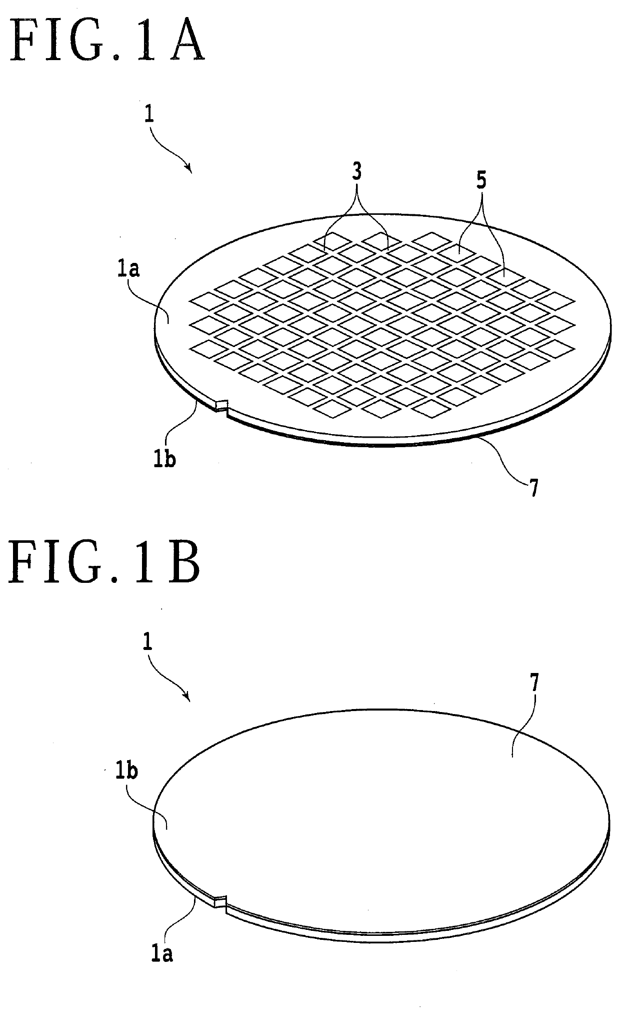
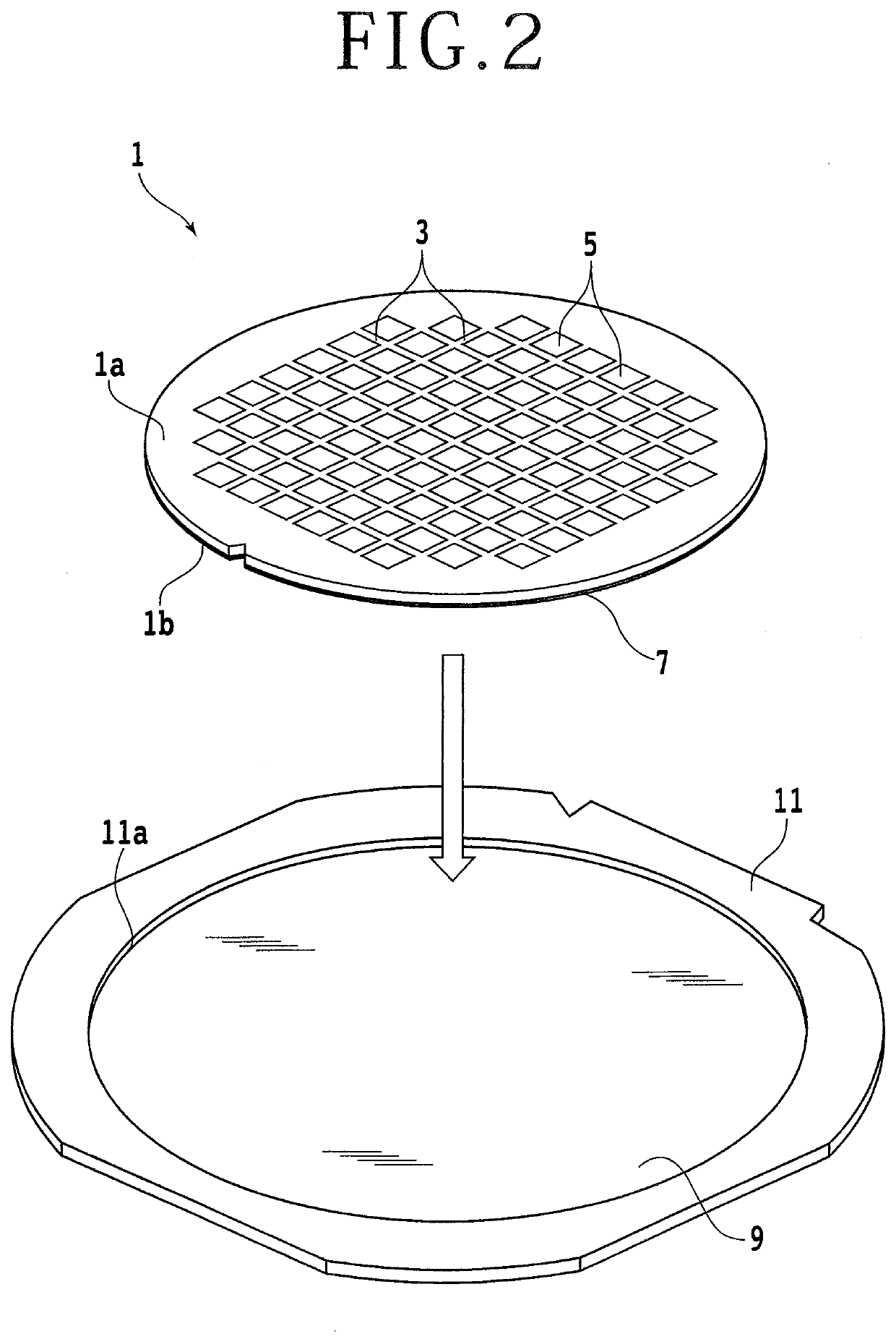
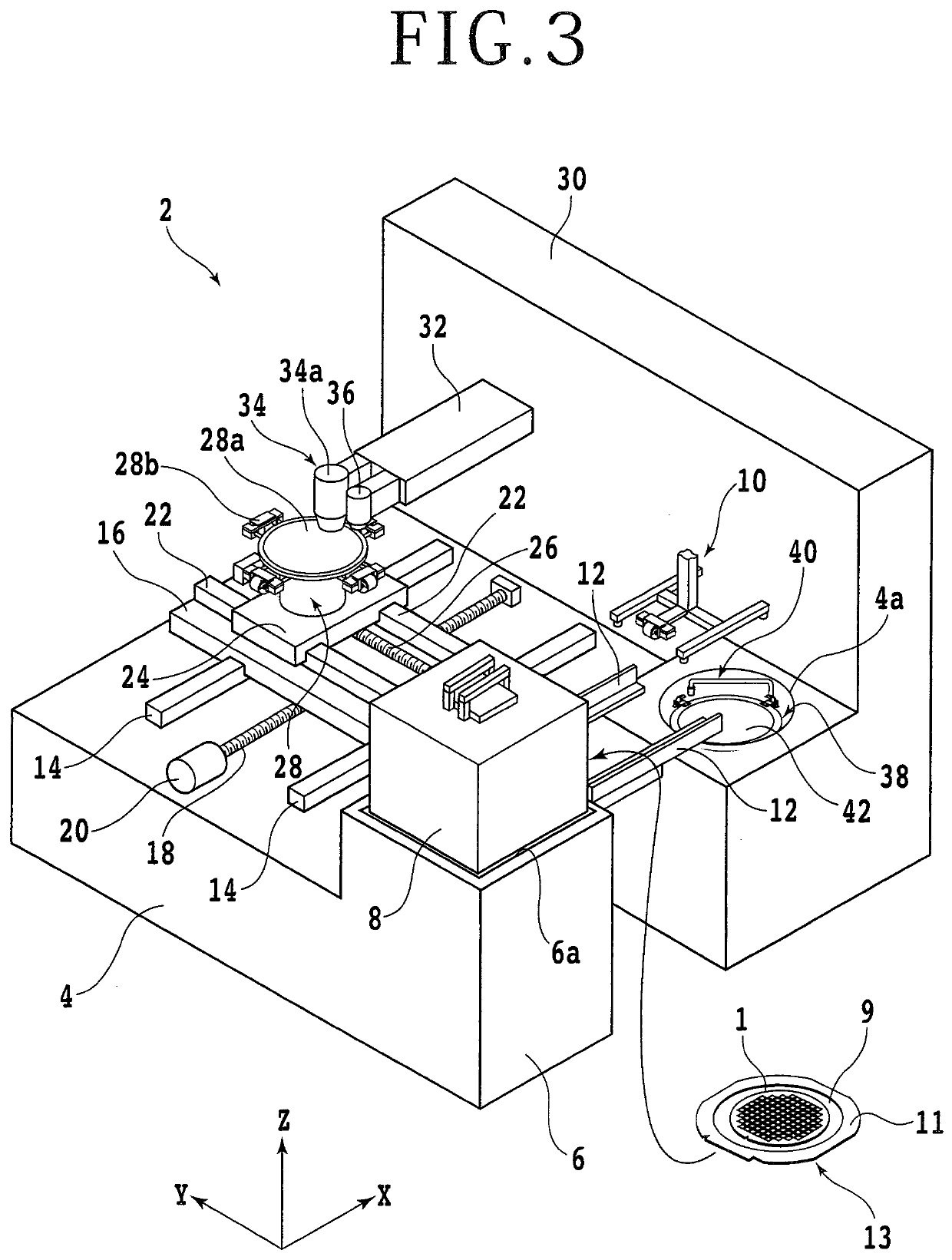
[0078]In a first example, description will be made of a case where a liquid resin soluble in an organic solvent is used as the protective film 40b. In the first example, description will be made of a case where a GaAs wafer 1 is set as a workpiece, the protective film 40b is formed on the top surface 1a of the wafer 1, and the wafer 1 is cut. In the first example, the frame unit preparing step S1 was performed to form the frame unit 13 by affixing a dicing tape “D765” manufactured by Lintec Corporation as the tape 9 to the undersurface 1b side of the wafer 1 having a metallic film formed on the undersurface 1b side. Next, in the protective film forming step S2, the top surface 1a side of the wafer 1 was coated with a liquid resin formed by dissolving polyvinyl butyral (PVB) in propylene glycol monomethyl ether (PGME). Solvent Black 3 as a light absorbing agent capable of absorbing light having a wavelength of 532 nm was added to the liquid resin in advance.

[0079]The protective film ...

second example

[0084]In a second example, description will be made of a case where a water-soluble liquid resin is used as the protective film 40b. In the second example, description will be made of a case where a GaAs wafer 1 is set as a workpiece, the protective film 40b is formed on the top surface 1a of the wafer 1, and the wafer 1 is cut. Incidentally, an oxide film is formed on the top surface 1a of the wafer 1. In the second example, as in the first example, the frame unit preparing step S1 was performed to form the frame unit 13 by affixing a dicing tape “D765” manufactured by Lintec Corporation as the tape 9 to the undersurface 1b side of the wafer 1 having a metallic film formed on the undersurface 1b side. Next, in the protective film forming step S2, the top surface 1a side of the wafer 1 was coated with “HogoMax003” of a water-soluble protective film material “HOGOMAX (registered trademark)” manufactured by DISCO Corporation as the liquid resin. The drying of the liquid resin, the cut...

third example

[0088]In a third example, description will be made of a case where the top surface 1a side of the wafer 1 is coated with a water-soluble liquid resin by performing the first coating step in the protective film forming step S2, and the top surface 1a side of the wafer 1 is next coated with a water-insoluble liquid resin by performing the second coating step. In the third example, description will be made of a case where a GaAs wafer 1 is set as a workpiece, the protective film 40b is formed on the top surface 1a of the wafer 1, and the wafer 1 is cut. In the third example, as in the first example and the second example, the frame unit preparing step S1 was performed to form the frame unit 13 by affixing a dicing tape “D765” manufactured by Lintec Corporation as the tape 9 to the undersurface 1b side of the wafer 1 having a metallic film formed on the undersurface 1b side.

[0089]Next, the protective film forming step S2 was performed. In the first coating step of the protective film fo...


PUM

PropertyMeasurementUnit
Electrical resistanceaaaaaaaaaa
Solubility (mass)aaaaaaaaaa
Metallic bondaaaaaaaaaa

Abstract

A method of processing a workpiece includes: a frame unit preparing step of preparing a frame unit including a tape affixed to an undersurface of the workpiece; a protective film forming step of forming a protective film on a top surface of the workpiece; a cutting step of cutting the workpiece by applying a laser beam; an interval expanding step of widening intervals between chips formed in the cutting step by expanding the tape outward in a radial direction; and an etching step of removing altered regions formed in the respective chips.

Description

BACKGROUND OF THE INVENTIONField of the Invention[0001]The present invention relates to a processing method of processing a workpiece such as a wafer formed of a semiconductor or the like, and a device chip manufacturing method of manufacturing device chips by processing the wafer.Description of the Related Art[0002]A plurality of intersecting planned dividing lines are set on the top surface of a disk-shaped wafer formed of a semiconductor, a device is formed in each of regions demarcated by the planned dividing lines, and device chips can be formed when the wafer is divided along the planned dividing lines. A cutting apparatus having an annular cutting blade, for example, is used when a wafer formed of a semiconductor material such as Si, GaAs, or the like having a plurality of devices formed on a top surface thereof is divided into each device (see Japanese Patent Laid-Open No. 2001-85365). The cutting apparatus cuts a workpiece by bringing the cutting blade being rotated into co...

Claims


Application Information

Patent Timeline
IPC IPC(8): H01L21/82H01L21/683H01L21/306H01L21/56
CPCH01L21/6836H01L21/56H01L21/82H01L21/30617H01L21/78H01L2221/6834H01L2221/68336H01L21/02076H01L21/76H01L24/50H01L21/30604H01L21/67092H01L21/67132H01S3/0007B23K26/38
Inventor NAKANO, KENTAKAWAGUCHI, HIDEYUKIIKEDA, YUKIYOSHIKAWA, TOSHIYUKIRYO, SENICHI
Owner DISCO CORP
Features
  • R&D
  • Intellectual Property
  • Life Sciences
  • Materials
  • Tech Scout
  • Unparalleled Data Quality
  • Higher Quality Content
  • 60% Fewer Hallucinations
Learn More