
Organic light emitting diode and organic light emitting device having the same

a light-emitting diode and organic technology, applied in the field of organic light-emitting diodes, can solve the problems of low luminous efficiency of common fluorescent materials and limited commercial applications, and achieve the effect of enhancing luminous efficiency and luminous lifetim

Active Publication Date: 2020-06-18
LG DISPLAY CO LTD
View PDF0 Cites 4 Cited by
  • Summary
  • Abstract
  • Description
  • Claims
  • Application Information

AI Technical Summary

Benefits of technology

The present disclosure aims to improve the efficiency and lifespan of organic light emitting diodes. The technical effects include reducing limitations and disadvantages of current technology. Additionally, the patent aims to enhance the brightness and duration of organic light emitting devices.

Problems solved by technology

Since only singlet excitons in the common fluorescent material according to the related art can be involved in luminous process, luminous efficiency of the common fluorescent material is low.
However, since a metal complex as a representative phosphorescent material has a short luminous lifetime, its commercial applications have been limited.

Method used


Image

  • Organic light emitting diode and organic light emitting device having the same
  • Organic light emitting diode and organic light emitting device having the same
  • Organic light emitting diode and organic light emitting device having the same

Examples


example 1

on of Organic Light Emitting Diode (OLED)

[0293]An organic light emitting diode was fabricated applying an exciton energy control layer (EEL) in an emitting material layer. An ITO (including reflective layer) attached glass substrate with 40 nm×40 nm×0.5 nm was ultrasonically cleaned with isopropyl alcohol, acetone and distilled water for 5 minutes and then dried in an oven at 100° C. The cleaned substrate was treated with O2 plasma in a vacuum for 2 minutes and transferred to a deposition chamber in order to deposit other layers on the substrate. An organic layer was deposited by evaporation by a heated boat under 10−7 torr in the following order. The deposition rate of the organic layer was set to 1 Å / s.

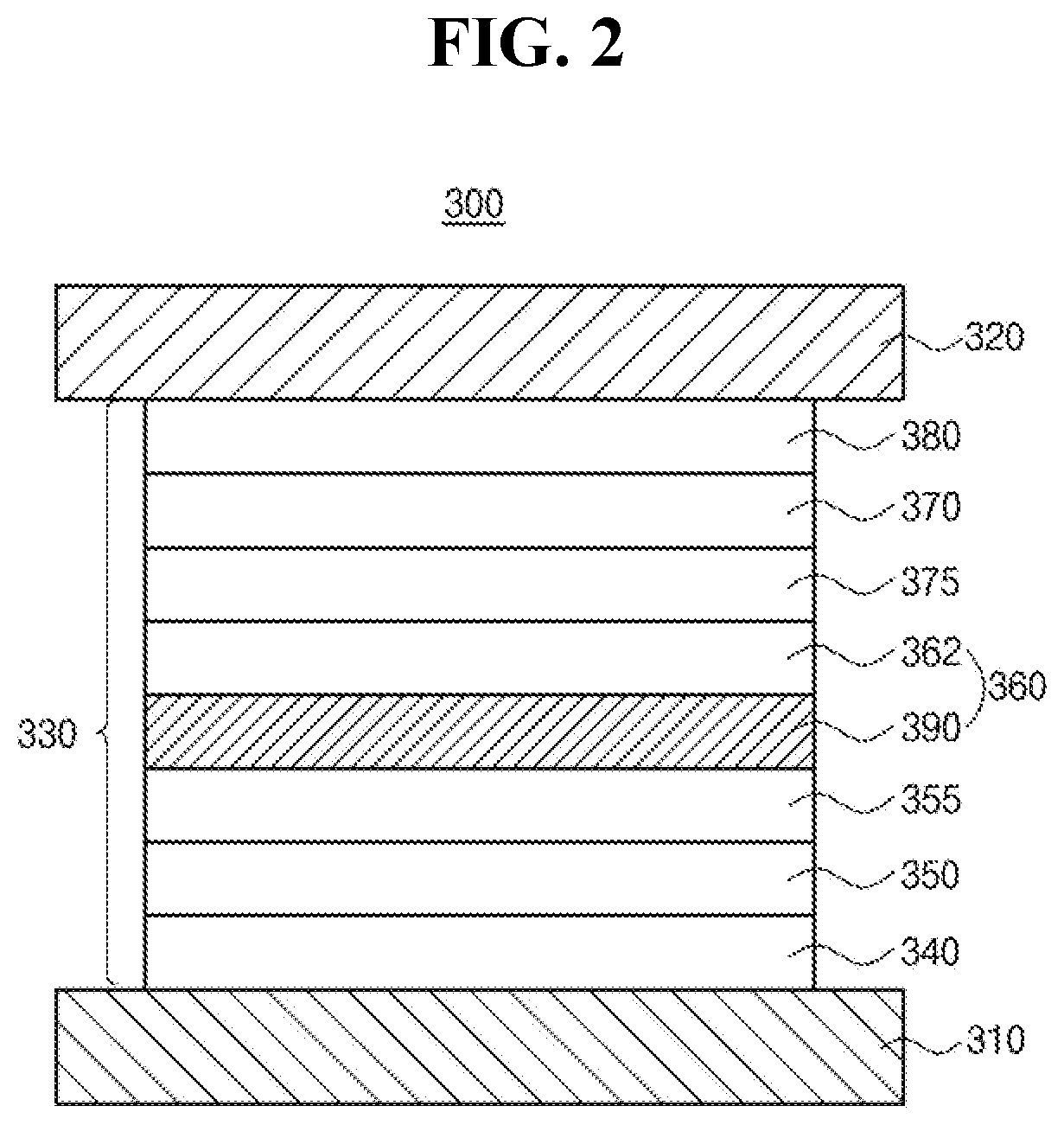
[0294]A hole injection layer (HIL) (HAT-CN; 50 Å); a hole transport layer (HTL) (NPB, 500˜1500 Å); an electron blocking layer (EBL) (TCTA; 50 Å); a first emitting material layer (EML1) (MADN (host): Compound 1 in Chemical Formula 3 (dopant)=70: 30; 60 Å); exciton energy control laye...

examples 4

n of OLED

[0297]An OLED was fabricated using the same materials as Example 1, except laminating sequentially the EML1 (MADN (host): Compound 1 in Chemical Formula 3 (dopant)=70: 30; 60 Å), a first exciton energy control layer (EEL1) (Compound 1; 10 to 20 Å), the EML2 (MADN(host): Compound 1 in Chemical Formula 3 (dopant)=70: 30; 70 Å), a second EEL (EEL2 (Compound 1; 10 to 20 Å), a third EML (EML3) (MADN (host): Compound 1 in Chemical Formula 3 (dopant)=70: 30; 130 Å) between the EBL and the ETL.

examples 5

n of OLED

[0298]An OLED was fabricated using the same materials as Example 4, except laminating the EML2 with a thickness of 140 Å and the EML3 with a thickness of 60 Å.


PUM


Abstract

An organic light emitting diode including at least one emitting material layer, which includes a host and a dopant and at least one exciton energy control layer disposed adjacently to the at least one emitting material layer and an organic light emitting device having the same is disclosed. The at least one exciton energy control layer includes an organic compound that has excited state singlet and triplet energy levels lower than excited state singlet and triplet energy levels of the host. The organic light emitting diode can enhance its luminous efficiency and its luminous lifetime by incorporating one or more exciton energy control layers.

Description

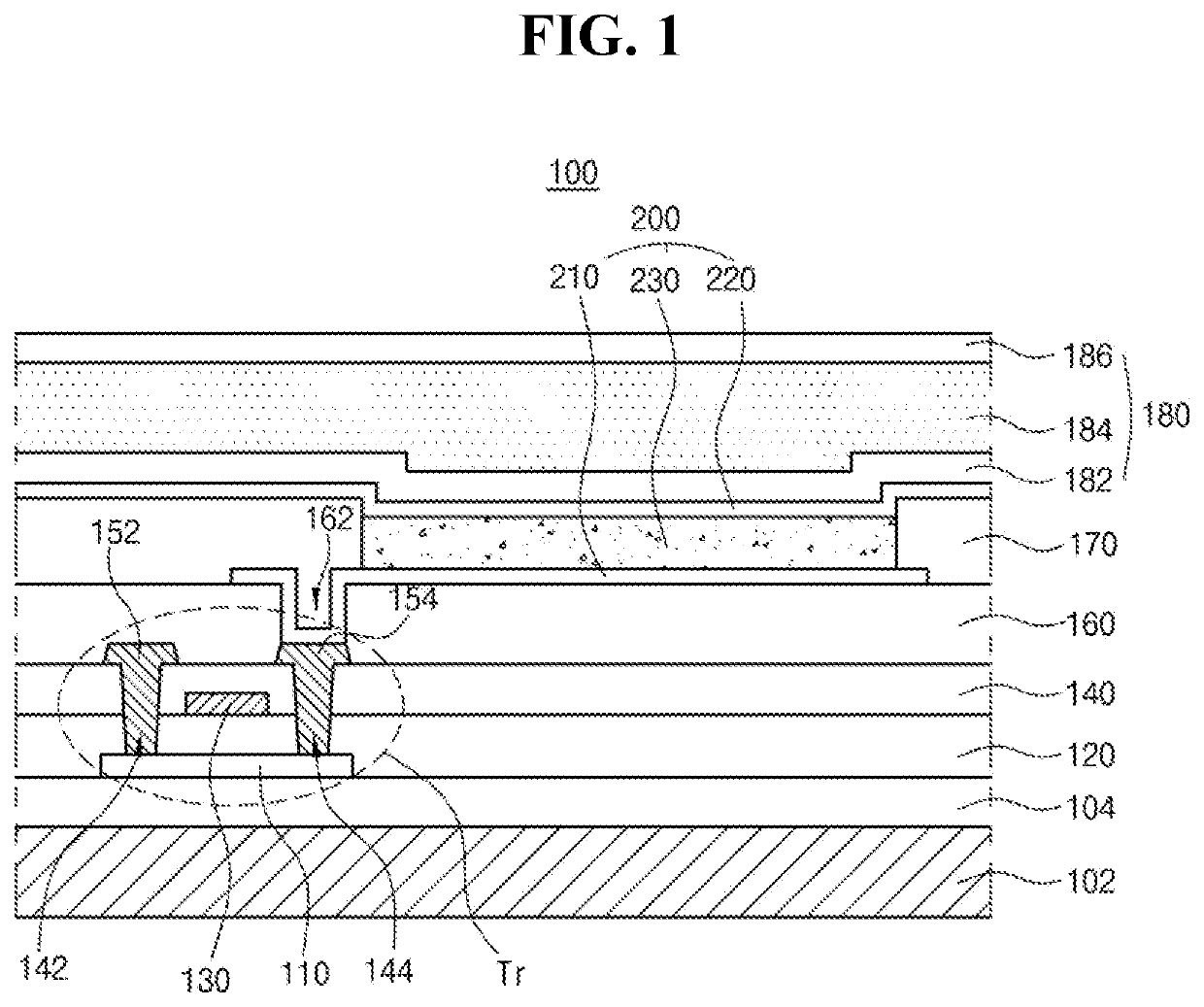
CROSS-REFERENCE TO RELATED APPLICATIONS[0001]This application claims the priority benefit under 35 U.S.C. § 119(a) of Korean Patent Application No. 10-2018-0161122, filed in the Republic of Korea on Dec. 13, 2018, which is incorporated herein by reference in its entirety into the present application.BACKGROUNDTechnical Field[0002]The present disclosure relates to an organic light emitting diode, and more specifically, to an organic light emitting diode having enhanced luminous efficiency and life span and an organic light emitting device having the same.Description of the Related Art[0003]Among the flat display devices used widely at present, organic light emitting diodes (OLEDs) are rapidly replacing liquid crystal display devices (LCDs). In the OLED, when electrical charges are injected into an emission layer between an electron injection electrode (i.e., cathode) and a hole injection electrode (i.e., anode), electrical charges are combined to be paired, and then emit light as the...

Claims


Application Information

Patent Timeline
IPC IPC(8): H01L51/00
CPCH01L51/0073H01L51/0074H01L51/0072H01L51/0067H10K59/12H10K50/121H10K50/12H10K50/11H10K2101/10H10K50/18H10K59/875C07D403/14C07D403/10C07D409/14C07D405/14H10K85/654H10K85/6572H10K2101/40H10K2101/20C09K11/06H10K85/657H10K85/6576H10K85/6574
Inventor SEO, BO-MINBAEK, JEONG-EUNYOON, DAE-WIYOO, MI-SANG
Owner LG DISPLAY CO LTD
Learn More