CuO/Se COMPOSITE FILM

a composite film and cuo technology, applied in the field of semiconductor materials, can solve the problems of severe carrier recombination, inability to prepare by vacuum thermal evaporation method, and inability to improve the crystallinity of cuo, so as to reduce the defect rate, and eliminate or reduce the defect of the cuo film

Active Publication Date: 2020-10-01
SHAANXI NORMAL UNIV
View PDF0 Cites 2 Cited by
  • Summary
  • Abstract
  • Description
  • Claims
  • Application Information

AI Technical Summary

Benefits of technology

[0016]In the invention, Se with a low melting point (221° C.) and strong photosensitivity is introduced into CuO, and then melt by low-temperature annealing (near the melting point of Se). The molten Se can infiltrate CuO to eliminate or reduce the defects in the CuO film such as voids and dangling bonds, providing the CuO / Se composite film with fewer defects. The composite film combines the merits of CuO such as strong light adsorption and suitable band gap with the merits of Se such as low melting point, low-temperature preparation and treatment and strong photosensitivity, simultaneously overcoming the shortcomings that CuO has high melting point and is decomposed at a high temperature and Se has too large band gap (about 1.8 eV). Thus, the film prepared herein has excellent optical, electrical and photoelectronic properties, having a brilliant application prospect in the fields of optoelectronic devices (including solar cells).

Problems solved by technology

), it can not be prepared by a vacuum thermal evaporation method, and the crystallinity of CuO can not be improved by a high-temperature annealing method.
However, the CuO film prepared by these methods has poor crystallinity and many defects, resulting in severe carrier recombination and poor device performance.

Method used


Image

  • CuO/Se COMPOSITE FILM
  • CuO/Se COMPOSITE FILM

Examples


example 1

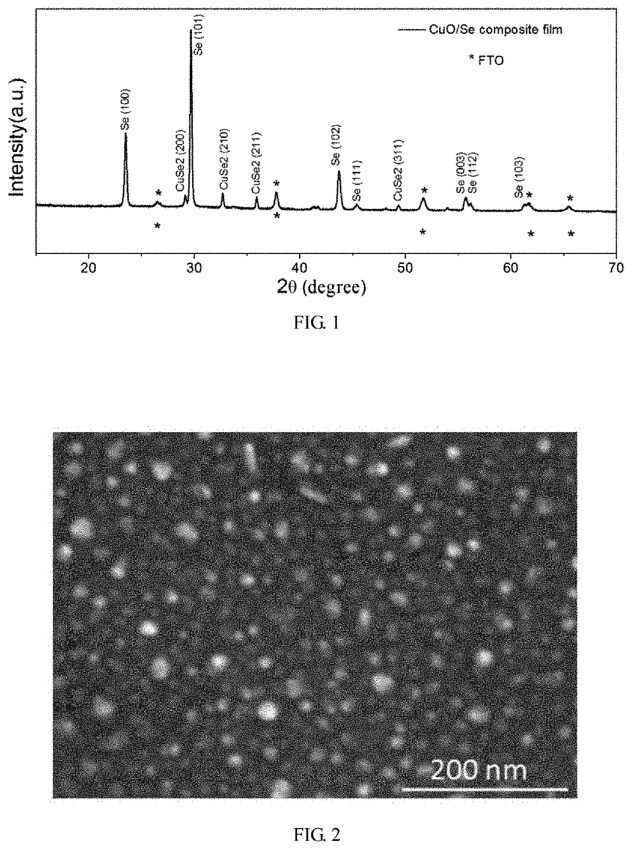
[0022]An ordinary glass substrate was cleaned sequentially in acetone, ethanol and deionized water under ultrasonication for 10 min, dried with nitrogen and then placed in a magnetron sputtering deposition chamber. The deposition chamber was vacuumed to 2×10⁻⁴ Pa using a mechanical pump and a turbomolecular pump, and a distance between the glass substrate and a target material was adjusted to 6 cm. Then the glass substrate was heated to 200° C. An argon vent valve was opened to fill the deposition chamber with argon. Simultaneously, a mass flow meter was opened to control the argon flow rate to 30 sccm. The pressure of the deposition chamber was adjusted to 0.6 Pa. CuO and Se were co-sputtered onto the rotated substrate under a sputtering power of 60 W for 30 min to deposit a composite film on the glass substrate, where the deposited composite film had a thickness of 4 μm. After that, the deposited composite film was naturally cooled to room temperature and annealed at 200° C. in th...

example 2

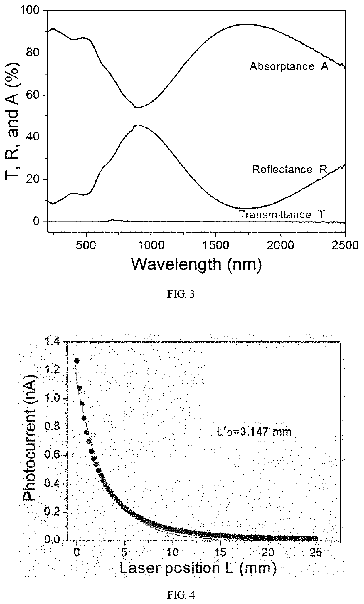
[0024]In this embodiment, CuO, Se and Si were co-sputtered to prepare a CuO / Se composite film according to the conditions of Example 1, where the atomic percentages of Cu, O, Se and Si in the CuO / Se composite film were 30%, 30%, 36% and 4%, respectively. The CuO / Se composite film prepared herein also showed strong absorption to light throughout the solar spectrum (250-2500 nm) with an average absorption rate close to 80%. The photo-generated carrier diffusion length LD of the CuO / Se composite film was directly measured by photocurrent scanning method to be 3.124 mm.

example 3

[0025]A CuO film was deposited by magnetron sputtering on a glass substrate according to the conditions of Example 1, and then a Se film was deposited on the CuO film by conventional thermal evaporation. Then the two layers of films were annealed at 220° C. in the air for 10 min to produce a CuO / Se composite film.


PUM

PropertyMeasurementUnit
optical band gapaaaaaaaaaa
melting pointaaaaaaaaaa

Abstract

Disclosed is a CuO/Se composite film, in which Se with low melting point (221° C.) and strong photosensitivity is introduced into CuO, providing the film with fewer defects and excellent optical, electrical and photoelectric properties. In the preparation method of the invention, Se is introduced into CuO and melted by low-temperature annealing, and then the molten Se can infiltrate CuO to eliminate or reduce defects in the CuO film such as voids and dangling bonds, thereby improving optical, electrical and photoelectric properties of the film and overcoming the shortcomings that CuO has poor crystallinity, high melting point and is decomposed at a high temperature.

Description

CROSS-REFERENCE TO RELATED APPLICATIONS[0001]This application claims the benefit of priority from Chinese Patent Application No. 201910244517.8, filed on Mar. 28, 2019. The content of the aforementioned application, including any intervening amendments thereto, is incorporated herein by reference in its entirety.TECHNICAL FIELD[0002]The application relates to semiconductor materials, and more particularly to a semiconductor cupric oxide / selenium (CuO / Se) composite film.BACKGROUND OF THE INVENTION[0003]Cupric oxide (CuO) is an important p-type semiconductor material, which has an optical band gap of approximately 1.4 eV and low price due to the vast available copper resources. Cupric oxide also has a wide range of applications in the superconducting, magnetic, catalyzing and gas sensing materials, as well as energy-storage and solar cells. Since CuO will be decomposed near its melting point (1026° C.), it can not be prepared by a vacuum thermal evaporation method, and the crystallini...

Claims


Application Information

Patent Timeline
Patent Type & Authority Applications(United States)
IPC IPC(8): C23C14/08C23C14/35C23C14/18C23C14/16H01L21/02
CPCC23C14/16H01L21/02422H01L21/02403C23C14/18H01L21/02631H01L21/02381H01L21/02554H01L21/02598C23C14/35C23C14/087C23C14/0036C23C14/0623C23C14/24C23C14/352H01L21/02565H01L21/02568H01L21/02579H01L21/02595
Inventor GAO, FEIGAO, RONGRONGLIU, HAOLIU, SHENGZHONG
Owner SHAANXI NORMAL UNIV
Why Eureka
Try Eureka